Last Updated or created 2022-08-17
For accessing the different components in computers you have to use the Address Bus.
In most 8 bits computers there are 16 address lines.
The CPU on a 6502 can access 65536 addresses (16 bit ). But most chips in the circuit have just a few address lines.
So the chip to use has to be selected using a CE (chip Enable) signal.
Old article i found on my fileserver from 1984
74 Series logic
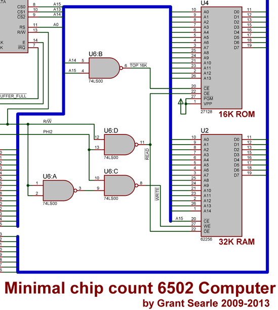
Above example uses A15 combined with A14 to address the 16K ROM
When using a 32k rom in the upper part of the memory, a15 can be used as CE
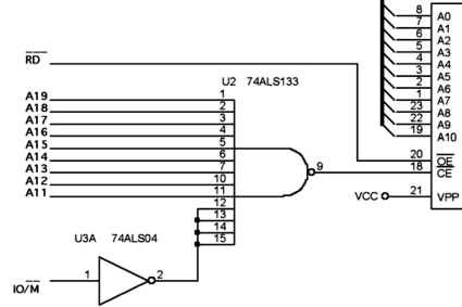
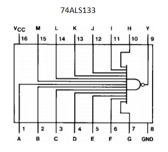
The 74ALS133 is a widely used decoder due to it’s many inputs.
Sometimes not all address lines are used for decoding, then you will get a repetition of the device in the memory map.
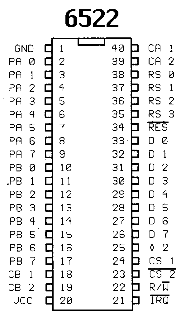
Above 6522 VIA has only 4 address lines RS0-RS3. But 2 chipselect pins (CS).
If you connect the chip as below.
A15 A14 A13 A12 A11 A10 A09 A08 A07 A06 A05 A04 A03 A02 A01 A00
CS1 CS2  NC  NC  NC  NC  NC  NC  NC  NC  NC  NC CR3 CR2 CR1 CR0
(NC - not connected, and CS2 is inverted!)
The chip would be selected when A15 is 1 and A14 is 0, A13-A04 it would not listen to. So its 4 bits addresses (total 16), would be repeated in a block $8000-$BFFF (10xx xxxx xxxx aaaa) 16384 addresses for 16 addresses on the 6522
ROM
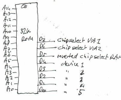
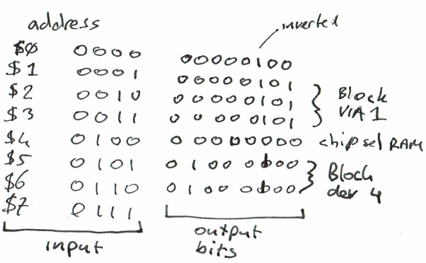
Another simple solution to get a more precise address decoder without using a lot of components is using a ROM.
But this wil only work for low speeds!
A eeprom is relative cheap
PAL PLA GAL
With these devices you can “program” a schematic which works as above example’s of the 74 series. But now you can do it using only one component.
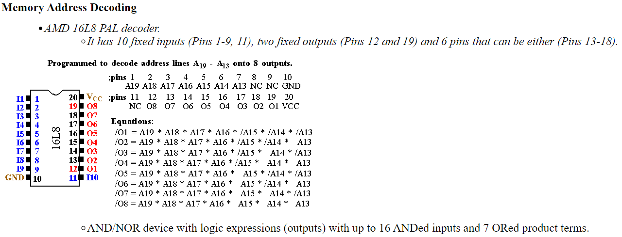
PALs and PLAs are fuse-programmed, some are erasable like (e)eprom.
Below a example of the code.
Most of the PAL/PLA/GAL are hard to get and obsolete
;PALASM Design Description
;---------------------------------- Declaration Segment ------------
TITLE    pRAM PC_interface Address Decoder
PATTERN  pRAM97A.pds
REVISION H
AUTHOR   Trevor Clarkson
COMPANY  EEE KCL
DATE     30/05/97

CHIP  decode  PALCE20V8

;---------------------------------- PIN Declarations ---------------
PIN  1          AEN                                   COMBINATORIAL ; INPUT
PIN  2          A9                                    COMBINATORIAL ; INPUT
PIN  3          A8                                    COMBINATORIAL ; INPUT
PIN  4          A7                                    COMBINATORIAL ; INPUT
PIN  5          A6                                    COMBINATORIAL ; INPUT
PIN  6          A5                                    COMBINATORIAL ; INPUT
PIN  7          A4                                    COMBINATORIAL ; INPUT
PIN  8          A3                                    COMBINATORIAL ; INPUT
PIN  9          A2                                    COMBINATORIAL ; INPUT
PIN  10         A1                                    COMBINATORIAL ; INPUT
PIN  11         IOW                                   COMBINATORIAL ; INPUT
PIN  12         GND
PIN  13         IOR                                   COMBINATORIAL ; INPUT
PIN  14         ACK_HALT                              COMBINATORIAL ; INPUT
PIN  15         PLS_EN                                COMBINATORIAL ; OUTPUT
PIN  16         BRDW                                  COMBINATORIAL ; OUTPUT
PIN  17         MOD_CTRL                              COMBINATORIAL ; OUTPUT
PIN  18         RAM_ACCESS                            COMBINATORIAL ; OUTPUT
PIN  19         IO_16                                 COMBINATORIAL ; OUTPUT
PIN  20         LATCH_MOD                             COMBINATORIAL ; OUTPUT
PIN  21         LATCH_ADD                             COMBINATORIAL ; OUTPUT
PIN  22         P300                                  COMBINATORIAL ; OUTPUT
PIN  23         P300IN                                COMBINATORIAL ; INPUT
PIN  24         VCC

;PC address decoding functions (not all in this PAL)
;uses latched address to provide low-order address lines to pRAM/RAM
;       A3      A2      A1      R/W     Addr    Function
;       0       0       0       R       300     MFF_0
;                               W               not used
;       0       0       1       R       302     MFF_1
;                               W               not used
;       0       1       0       R       304     MFF_2
;                               W               not used
;       0       1       1       R       306     MFF_3
;                               W               Latch Module Number
;       1       0       0       R       308     PLS_Status  (pRAM status)
;                               W               PLS_Control (pRAM control)
;       1       0       1       R       30A     Weight/Connection-
;                               W                Pointer RAM access
;       1       1       0       R       30C     not used
;                               W               Latched RAM address
;       1       1       1       R       30E     not used
;                               W               pRAM_256 module control
;
; NB. IO_16 must be tri-stated when not in use

;----------------------------------- Boolean Equation Segment ------
EQUATIONS

/P300 = A9*A8*/A7*/A6*/A5*/A4*/IOR + A9*A8*/A7*/A6*/A5*/A4*/IOW

/BRDW = /P300IN * /IOW

/PLS_EN = /P300IN*/A3*/IOR + /P300IN*A3*/A2*/A1

; MOD_CTRL is active HIGH
MOD_CTRL = ACK_HALT * /BRDW * A3 * A2 * A1 * /IOW

; RAM_ACCESS is active HIGH
RAM_ACCESS = ACK_HALT * /P300IN * A3 * /A2 * A1

IO_16 = GND
IO_16.TRST = /P300IN
; enable 16-bit transfers

; LATCH_MOD is active HIGH
LATCH_MOD = /BRDW * /A3 * A2 * A1

; LATCH_ADD is active HIGH
LATCH_ADD = /BRDW * A3 * A2 * /A1

;----------------------------------- Simulation Segment ------------
SIMULATION
TRACE_ON A9 A8 A7 A6 A5 A4 IOR /IOW /BRDW /PLS_EN MOD_CTRL RAM_ACCESS IO_16 LATCH_MOD LATCH_ADD ACK_HALT /P300 /P300IN
SETF /A9 /A8 /A7 /A6 /A5 /A4 /A3 /A2 /A1 IOR IOW /ACK_HALT /P300IN
SETF /IOW ; test P300 doesn't respond
SETF IOW /IOR ; test P300 doesn't respond
SETF IOR
SETF A9 A8 /A7 /A6 /A5 /A4 /IOR /P300IN
SETF A1
SETF A2 /A1
SETF A1 ; read mff0-3
SETF IOR /IOW ; test P300 and BRDW
SETF /A3 A2 A1 ; test Latch Module No
SETF IOW A3 A2 A1 ; MOD-CTRL not active until ACK_HALT
SETF ACK_HALT /IOW
SETF IOW /ACK_HALT
SETF A3 /A2 A1 ; check RAM_ACCESS
SETF ACK_HALT /IOW
SETF /ACK_HALT IOW
SETF ACK_HALT /IOR ; check READ and WRITE to RAM
SETF IOR P300IN
SETF /A3 A2 A1
SETF /ACK_HALT /P300IN
SETF IOW
SETF /A3 A2 A1 /IOW ; check LATCH_MOD
SETF IOW
SETF A3 A2 /A1
SETF /IOW       ; check LATCH_ADD
SETF /A3 /A2 /A1 ; shouldn't happen normally

TRACE_OFF
;-------------------------------------------------------------------
FPGA
Example FPGA code. A solution which is too fancy for my 6502.// Verilog code for decoder
// 5-input AND gate
module AND_5_input(g,a,b,c,d,e);
output g;
input a,b,c,d,e;
and #(50) and1(f1,a,b,c,d),
and2(g,f1,e);
endmodule
// fpga4student.com: FPGA projects, Verilog projects, VHDL projects
// Verilog code for decoder
// Decoder top level Verilog code using 5-input AND gates
module dec5to32(Out,Adr);
input [4:0] Adr; // Adr=Address of register
output [31:0] Out;
not #(50) Inv4(Nota, Adr[4]);
not #(50) Inv3(Notb, Adr[3]);
not #(50) Inv2(Notc, Adr[2]);
not #(50) Inv1(Notd, Adr[1]);
not #(50) Inv0(Note, Adr[0]);
AND_5_input a0(Out[0], Nota,Notb,Notc,Notd,Note); // 00000
AND_5_input a1(Out[1], Nota,Notb,Notc,Notd,Adr[0]); // 00001
AND_5_input a2(Out[2], Nota,Notb,Notc,Adr[1],Note); //00010
AND_5_input a3(Out[3], Nota,Notb,Notc,Adr[1],Adr[0]);
AND_5_input a4(Out[4], Nota,Notb,Adr[2],Notd,Note);
AND_5_input a5(Out[5], Nota,Notb,Adr[2],Notd,Adr[0]);
AND_5_input a6(Out[6], Nota,Notb,Adr[2],Adr[1],Note);
AND_5_input a7(Out[7], Nota,Notb,Adr[2],Adr[1],Adr[0]);
AND_5_input a8(Out[8], Nota,Adr[3],Notc,Notd,Note);
AND_5_input a9(Out[9], Nota,Adr[3],Notc,Notd,Adr[0]);
AND_5_input a10(Out[10], Nota,Adr[3],Notc,Adr[1],Note);
AND_5_input a11(Out[11], Nota,Adr[3],Notc,Adr[1],Adr[0]);
AND_5_input a12(Out[12], Nota,Adr[3],Adr[2],Notd,Note);
AND_5_input a13(Out[13], Nota,Adr[3],Adr[2],Notd,Adr[0]);
AND_5_input a14(Out[14], Nota,Adr[3],Adr[2],Adr[1],Note);
AND_5_input a15(Out[15], Nota,Adr[3],Adr[2],Adr[1],Adr[0]);
AND_5_input a16(Out[16], Adr[4],Notb,Notc,Notd,Note);
AND_5_input a17(Out[17], Adr[4],Notb,Notc,Notd,Adr[0]);
AND_5_input a18(Out[18], Adr[4],Notb,Notc,Adr[1],Note);
AND_5_input a19(Out[19], Adr[4],Notb,Notc,Adr[1],Adr[0]);
AND_5_input a20(Out[20], Adr[4],Notb,Adr[2],Notd,Note);
AND_5_input a21(Out[21], Adr[4],Notb,Adr[2],Notd,Adr[0]);
AND_5_input a22(Out[22], Adr[4],Notb,Adr[2],Adr[1],Note);
AND_5_input a23(Out[23], Adr[4],Notb,Adr[2],Adr[1],Adr[0]);
AND_5_input a24(Out[24], Adr[4],Adr[3],Notc,Notd,Note);
AND_5_input a25(Out[25], Adr[4],Adr[3],Notc,Notd,Adr[0]);
AND_5_input a26(Out[26], Adr[4],Adr[3],Notc,Adr[1],Note);
AND_5_input a27(Out[27], Adr[4],Adr[3],Notc,Adr[1],Adr[0]);
AND_5_input a28(Out[28], Adr[4],Adr[3],Adr[2],Notd,Note);
AND_5_input a29(Out[29], Adr[4],Adr[3],Adr[2],Notd,Adr[0]);
AND_5_input a30(Out[30], Adr[4],Adr[3],Adr[2],Adr[1],Note);
AND_5_input a31(Out[31], Adr[4],Adr[3],Adr[2],Adr[1],Adr[0]); // 11111
endmodule
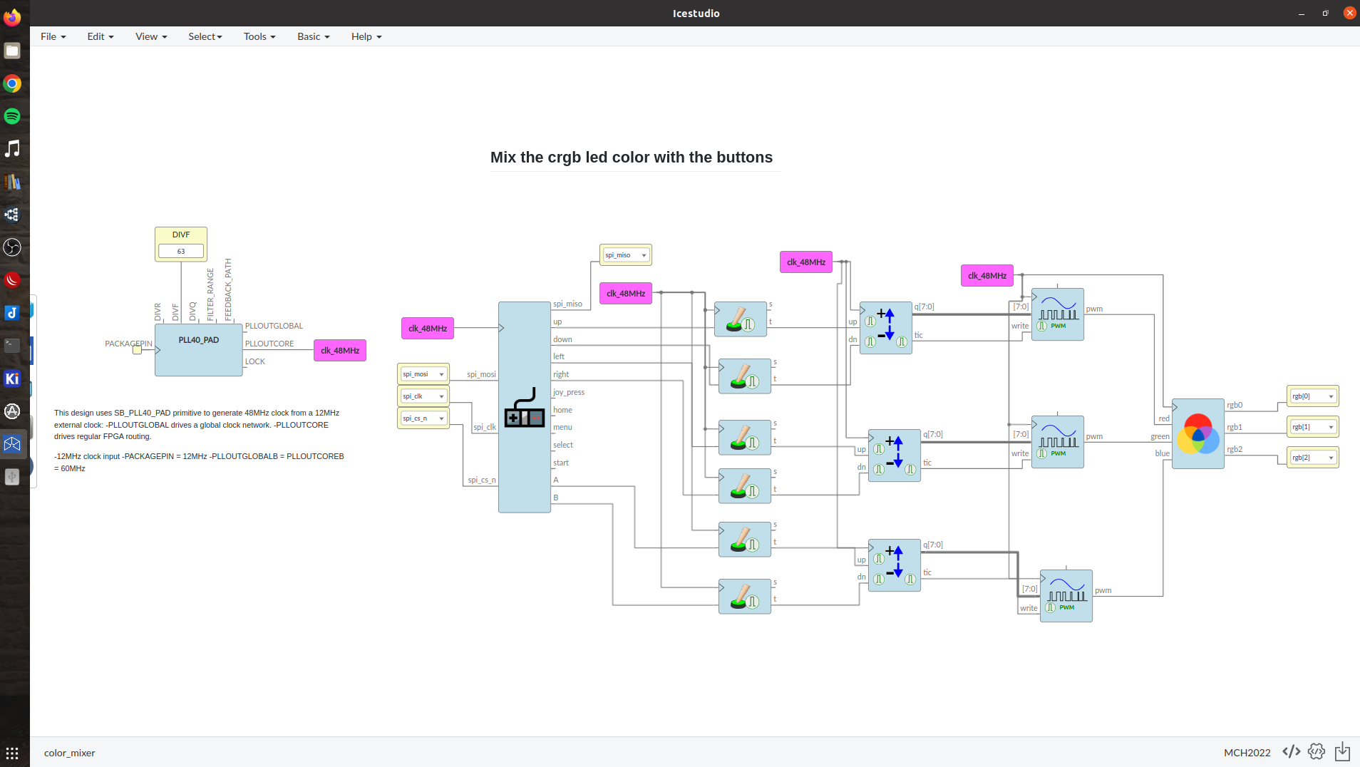
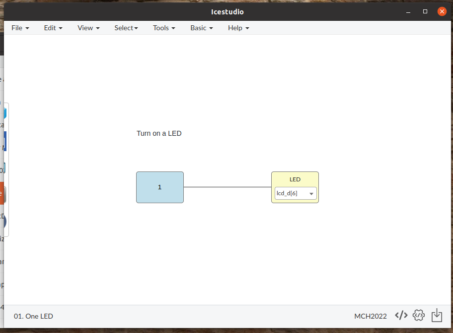
Example of Ice studio FPGA programming
Conslusion:
For now i will use the 74 logic. But i definitely will revisit FPGA’s