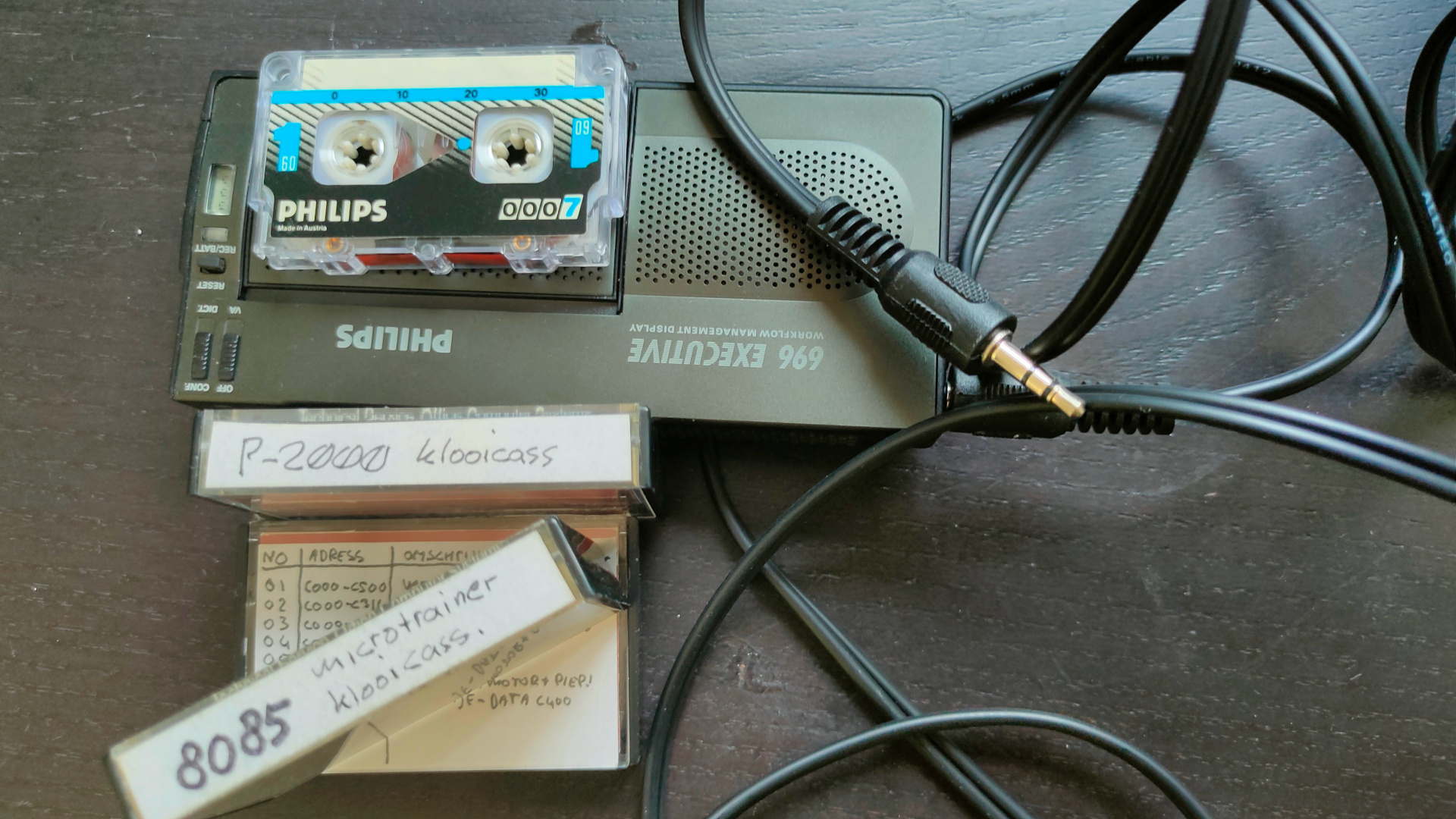
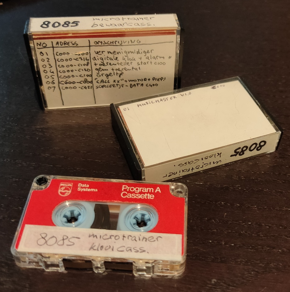
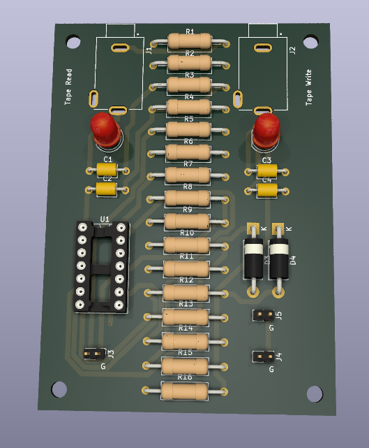
Started drawing a Cassette interface in Kicad. This so i can read back my old cassettes with programs. (And write some new stuff)
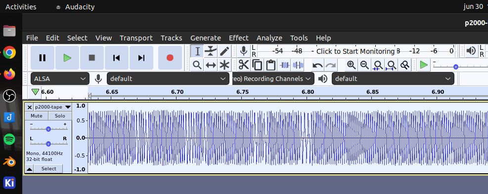
I’m planning to buy a small micro cassette player. With schematic below, I’m going to use it as save/load device. But also with the same player, I’m going to convert the tape to a wave file, and try to decode the program using python.
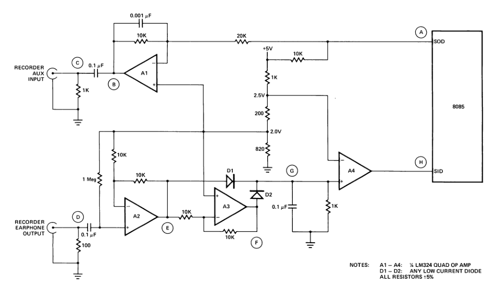
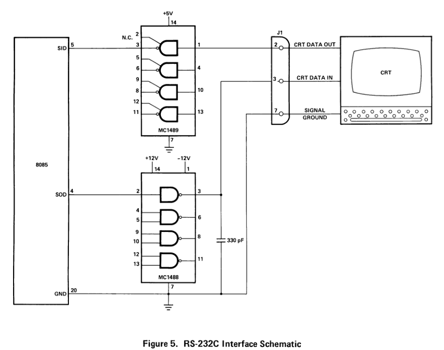
While I’m at it, reading the old manuals, a RS-232 interface would be nice also!
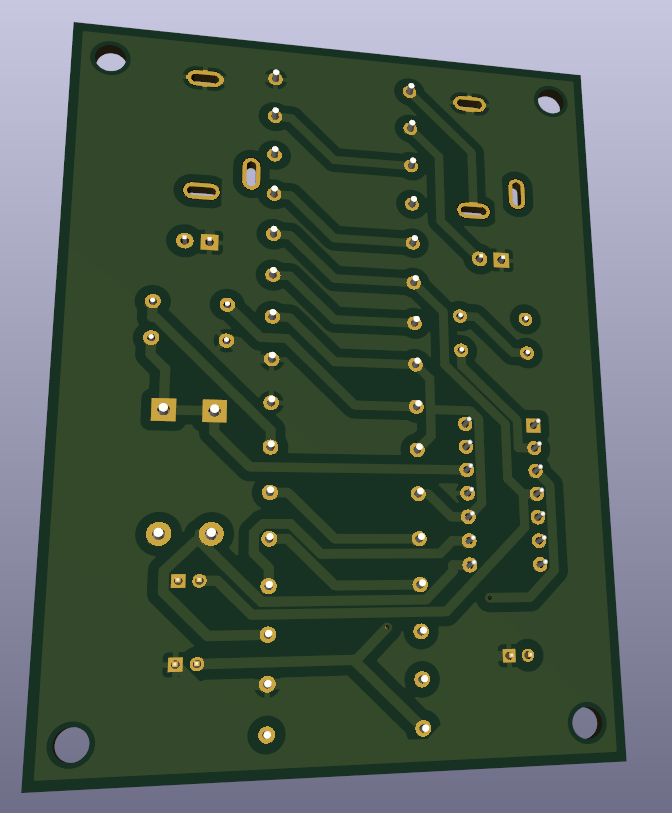
UPDATE 20231016
This is the final version
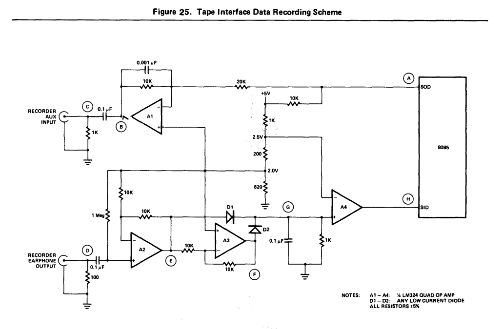
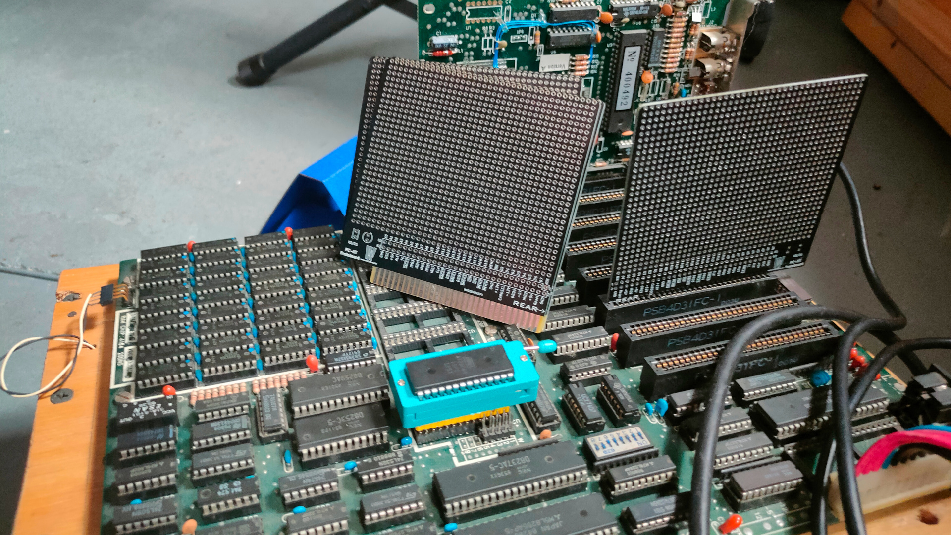
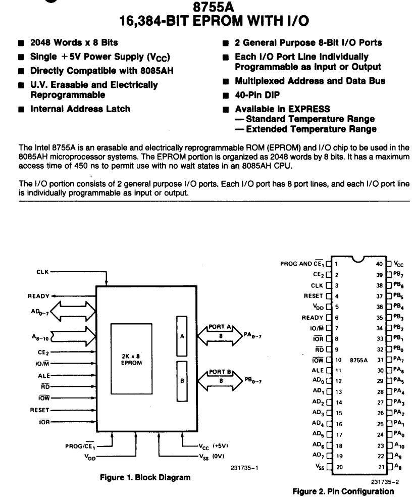
Information about the 7655A. A eprom WITH IO ports! Amazing piece of history hardware.
While working on my game, i had to come up with some solutions i could not find an answer for on the internet.
I’m not going to post every little detail of my game on this blog, my main reason is sharing my experiences and solutions.
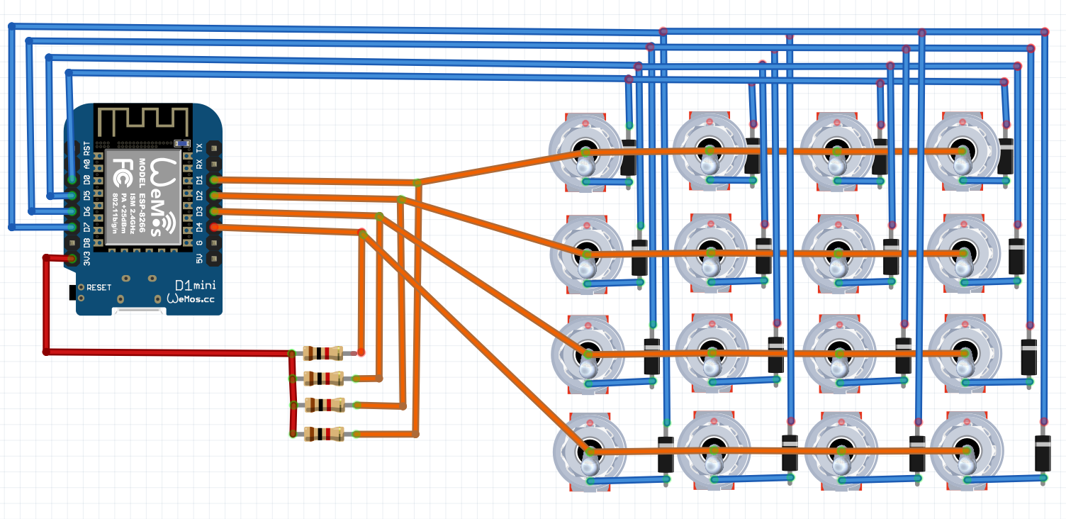
16 SWITCHES
16 Switches on a Wemos Arduino. While push buttons are easier to connect, I needed ON/OFF switches. Push buttons are easy, there is only one active, so 4 enable lines and 4 scan lines and you’re golden. 16 Switches can be enabled all at the same time. So you need some extra components to get a good result (0-65535)
Above schematic works, you need 4x 1k Pull-up resistors and 16 diodes. I used 1N4007
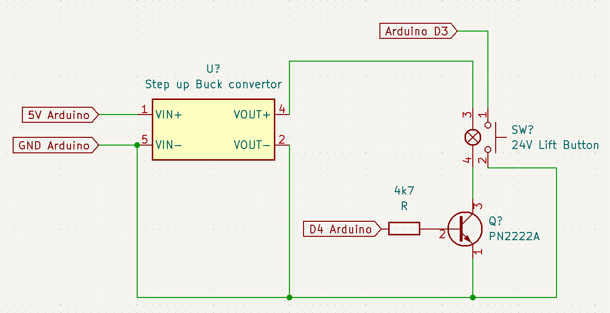
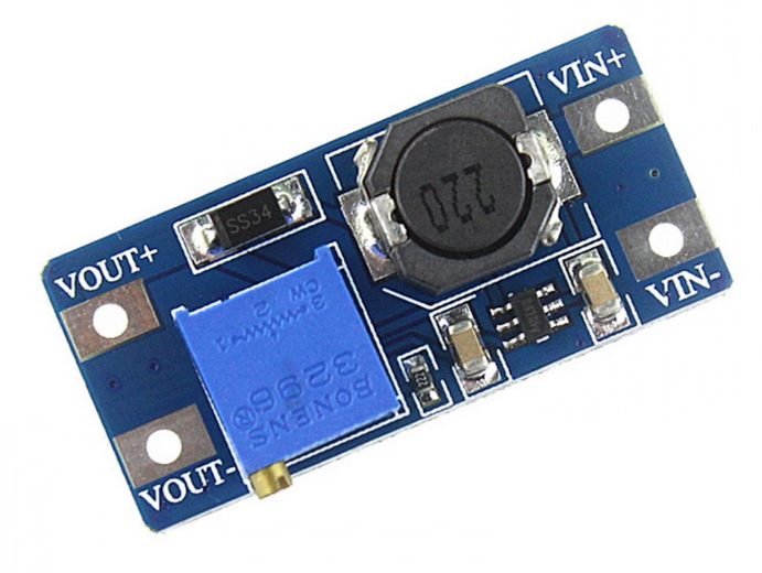
CONTROLLING 24V using Arduino and a buck convertor
Next problem, i’m using some elevator buttons for a project. These have build-in leds but run at 24V. I only have 5V from the Arduino. Regular leds you can connect directly to the Arduino using a 220ohm resistor. So i used a Buck-Step-Up-Convertor. This little module converts 5V to 24V. (You can control the output voltage using a variable resistor) To control the lamp/leds i used a PN2222a transistor to switch the lights on/off using a pin of the Arduino.
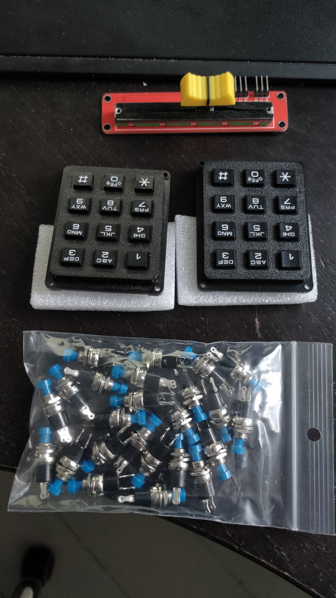
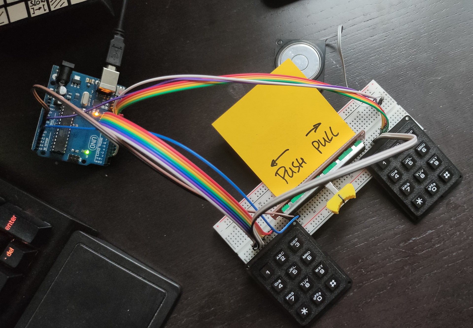
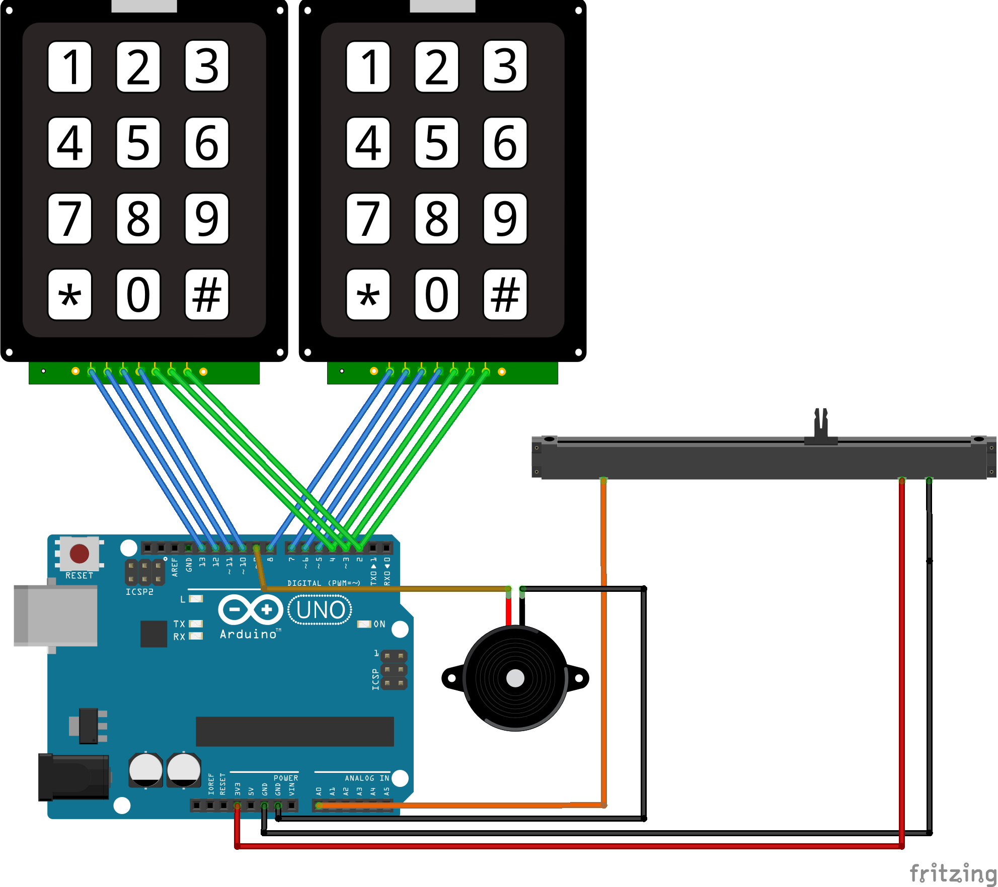
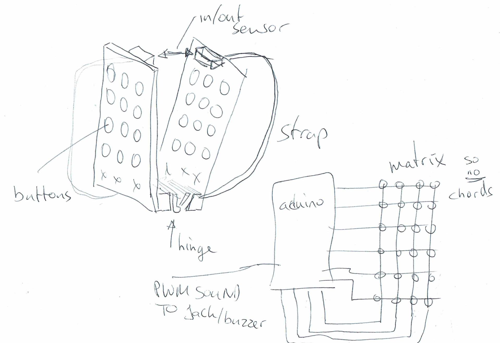
So we need some pushbuttons … at least 14 .. for the most simple tunes. A sensor for push and pull. A buzzer or better yet .. a jack for earphones. Arduino with enough pins to connect a keyboard matrix. When using a keyboard matrix only single keypresses are detected. So we cant do chords!
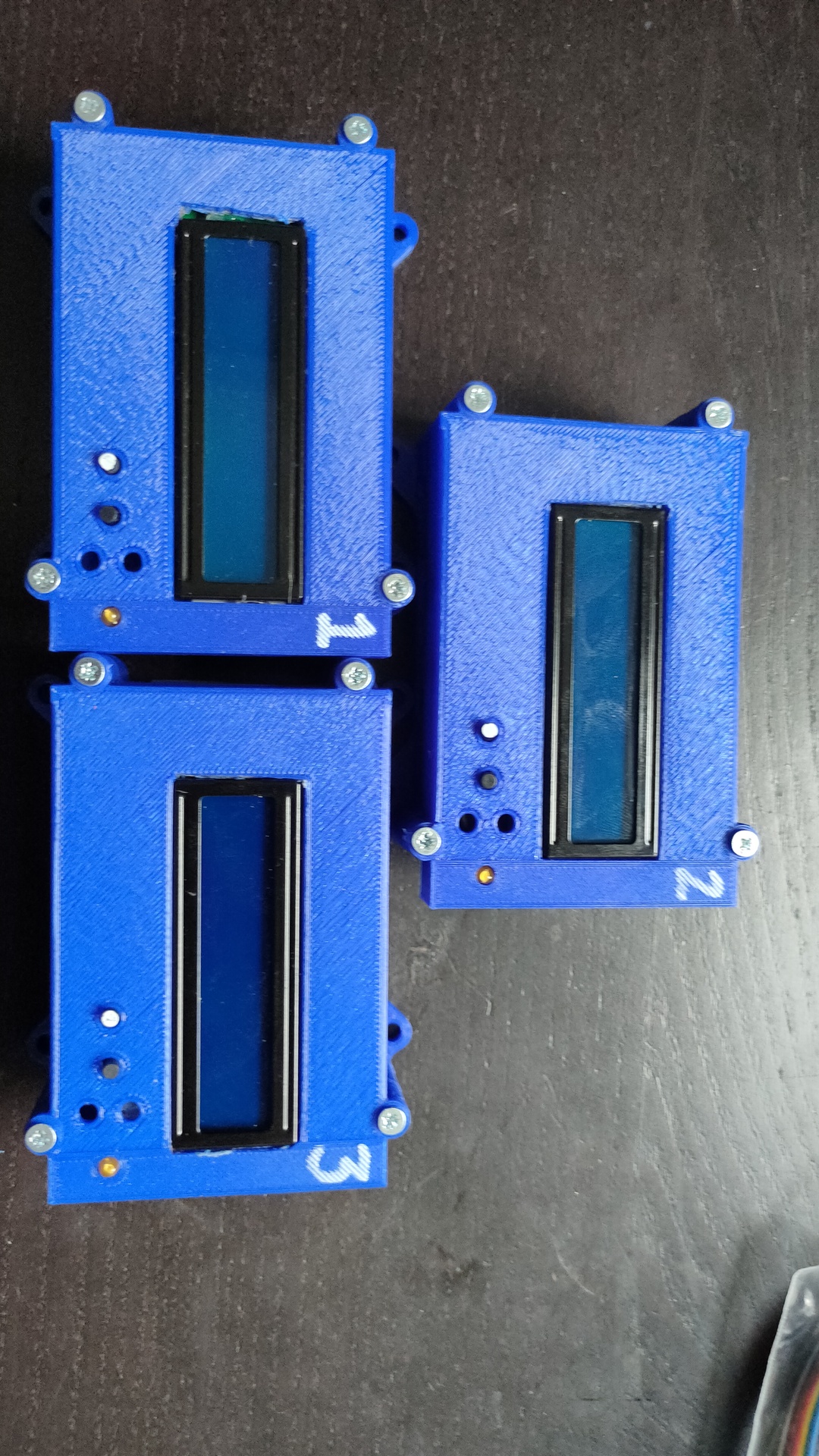
I’ve been working on some modular gadgets which can be combined to make a complete puzzle.
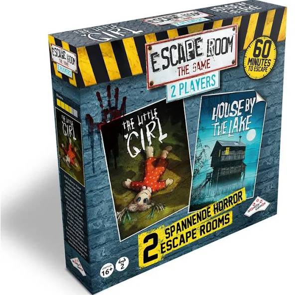
I like games like Keep-talking-and-nobody-dies. (Which is a computer game, but you have to play it with multiple persons and a physical “manual” Great fun!) https://keeptalkinggame.com/
And i like real escape rooms. There are some puzzle “rooms” you can buy in the game store, it is okay but many are for single use only.
I’ve been following some people on youtube, i saw some great ideas but not a remote over the internet using physical knobs and switches.
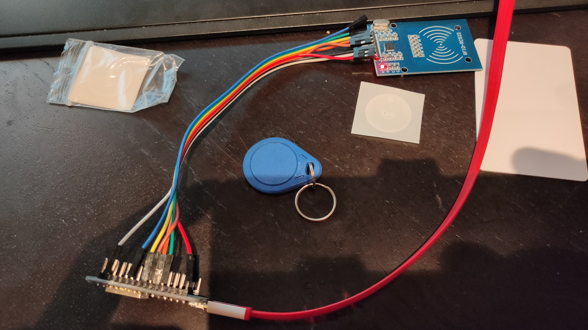
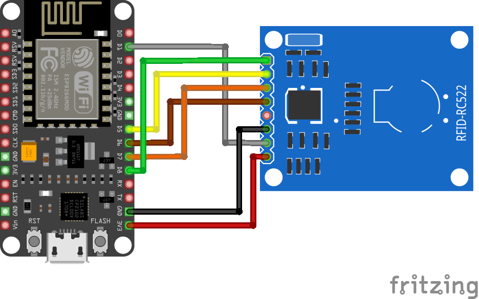
This is a RFID reader with an old Amico Esp8266 Arduino. It sends RFID information to the MQTT broker
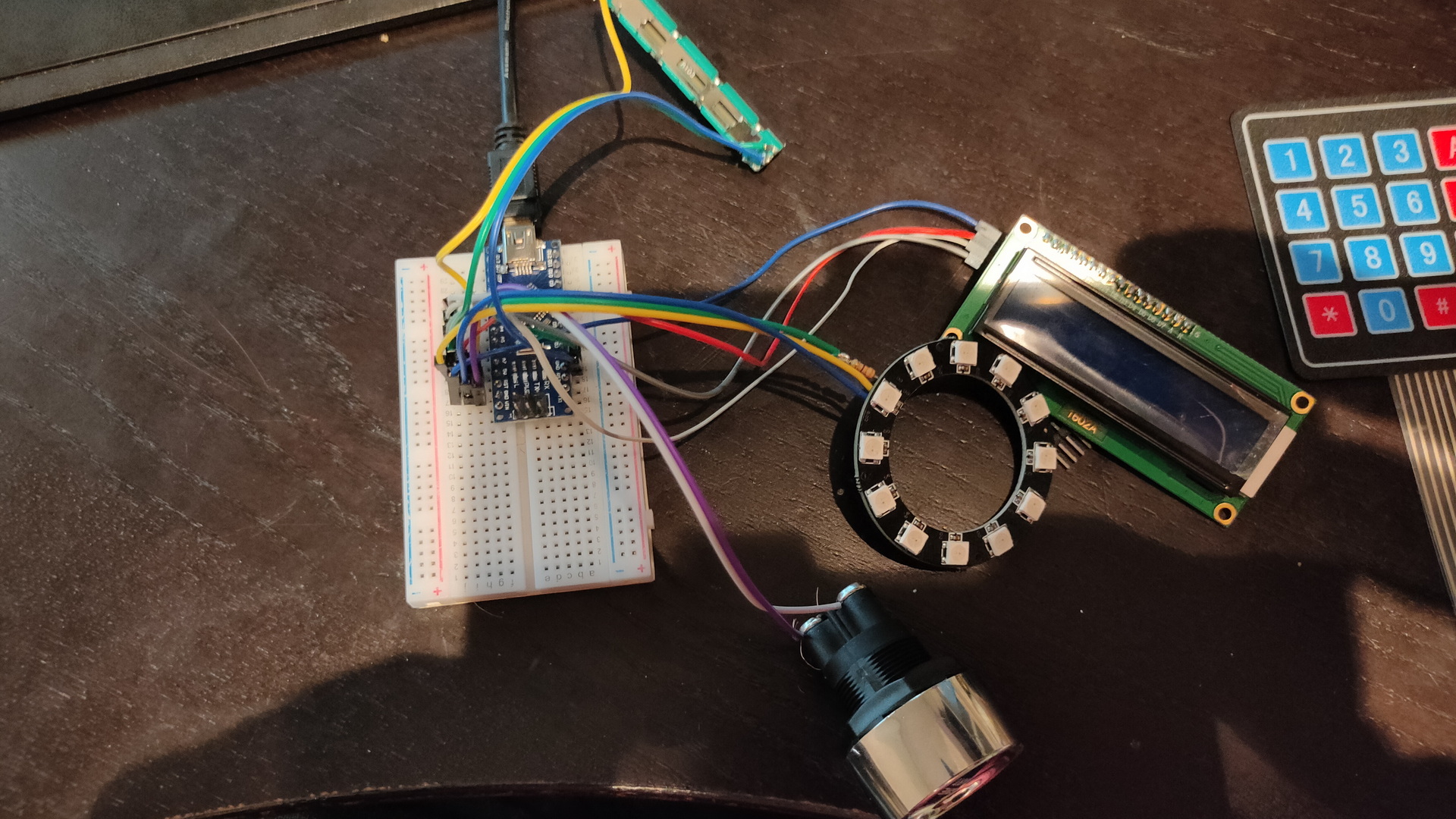
Some other tools ‘n knobs .. and stuff
I want to use Adhoc Wifi and a Mqtt/Nodered setup which uses a mqtt over the internet to get people (and their knobs) connected
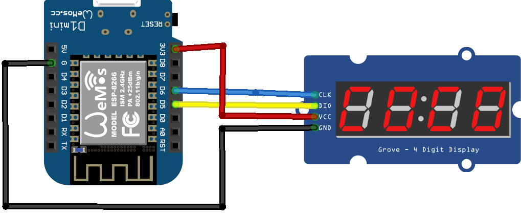
I already got a lot of test schematics
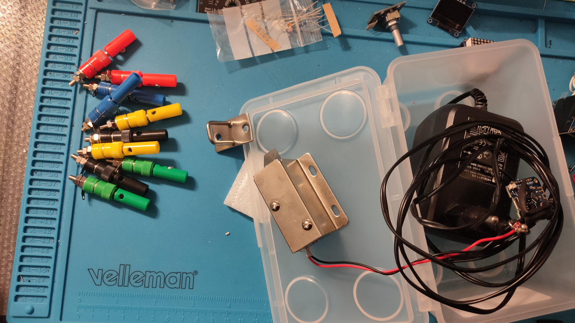
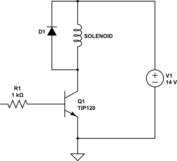
Left part of the “connect the wires puzzle” right a solenoid electrical lock)