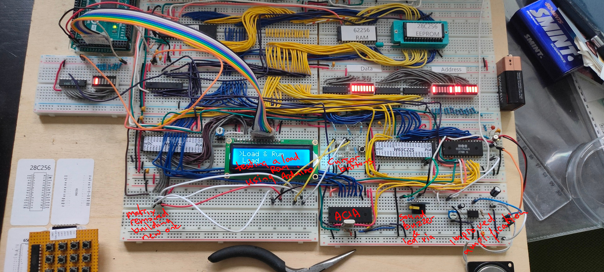
- New amplifier part using a LM386
- Buzzer and led on VIA 2, blinky and sound timed by the internal timers of the 6522
- ACIA testing still going on, writing software
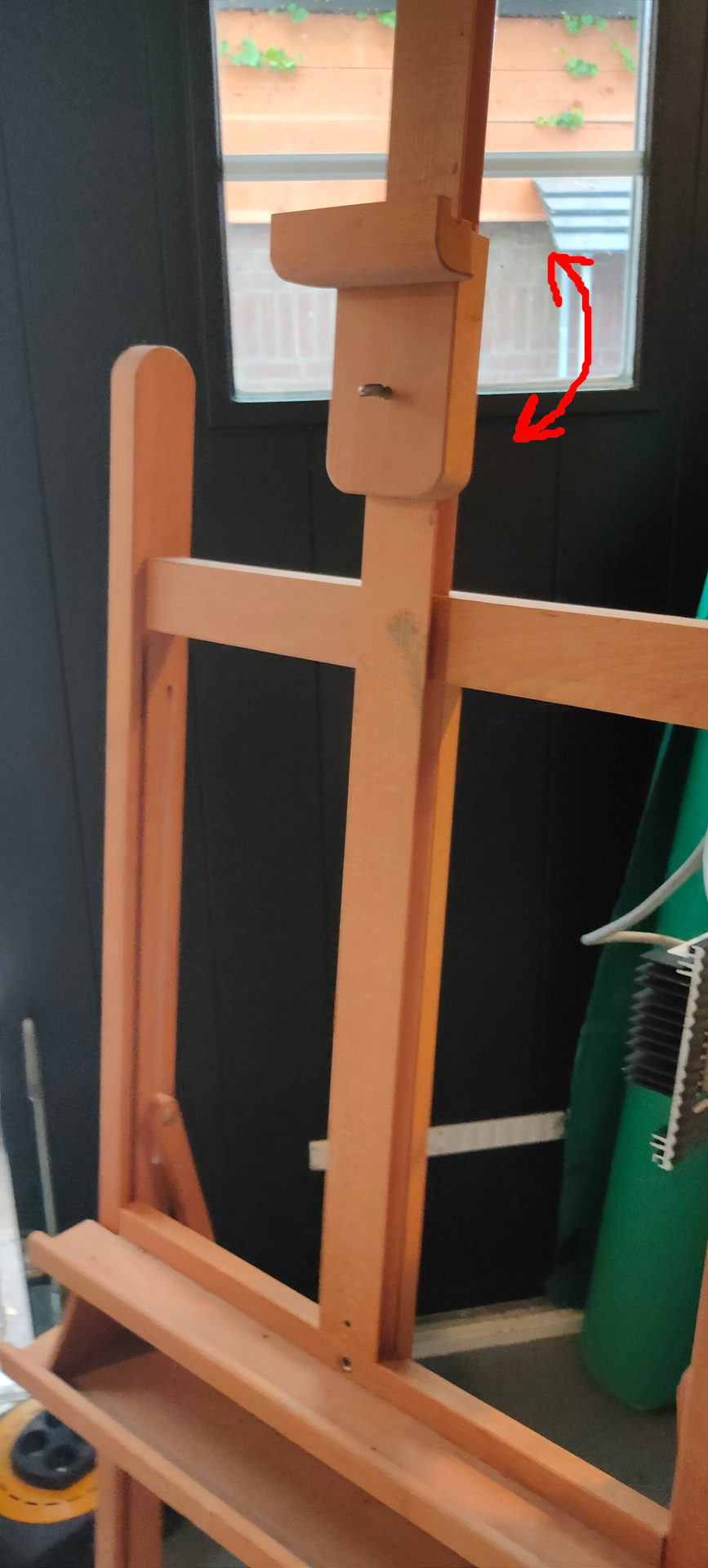
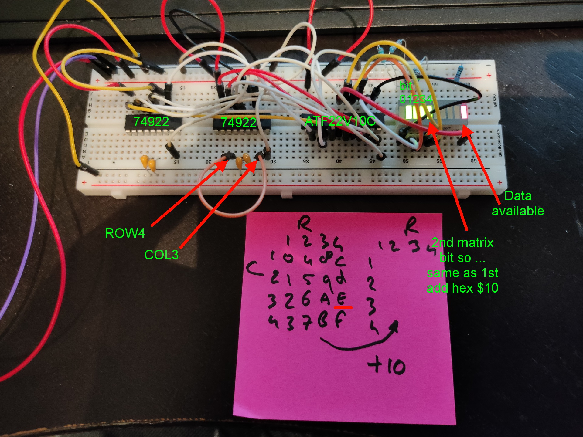
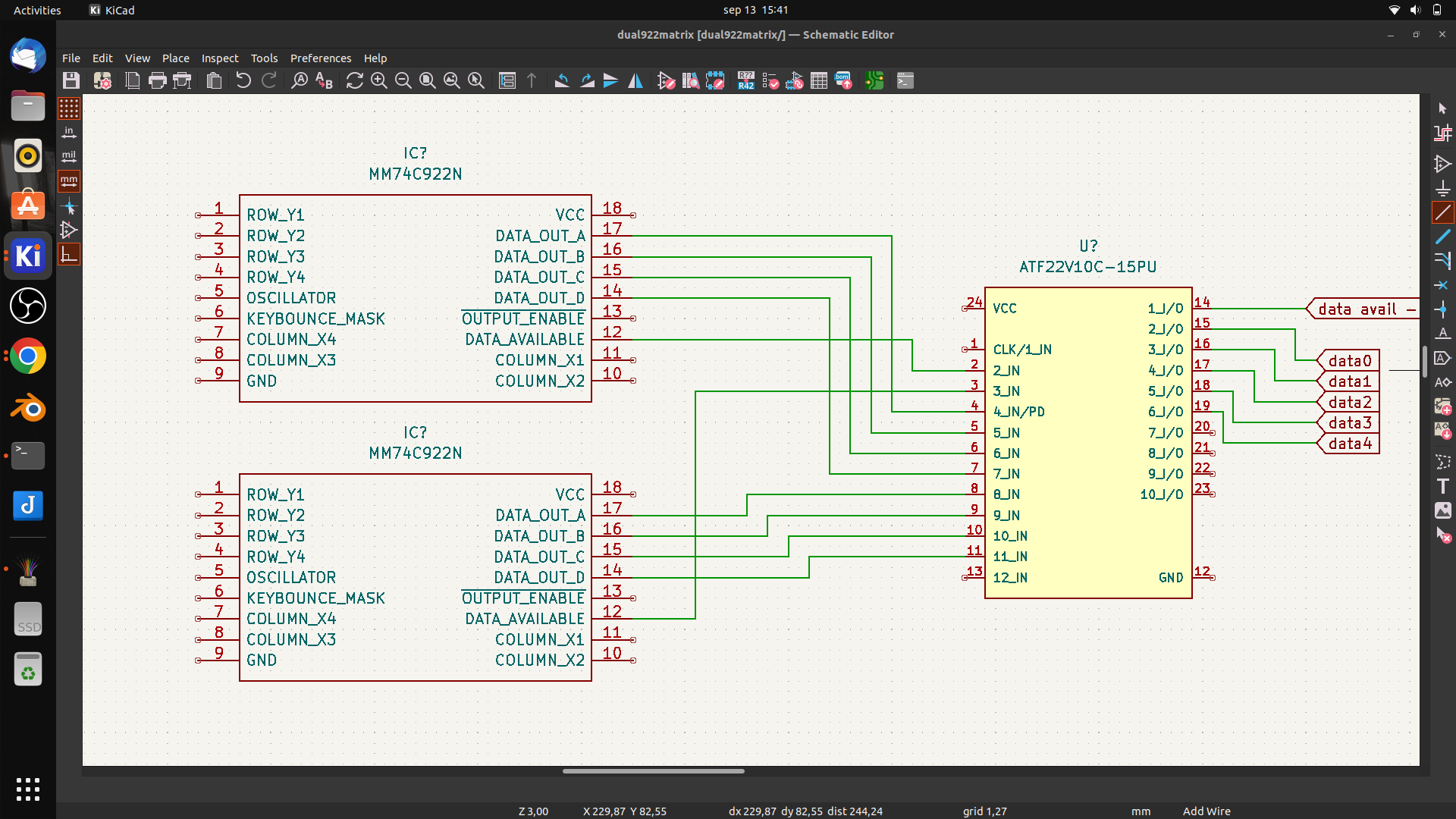
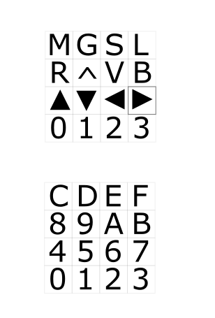
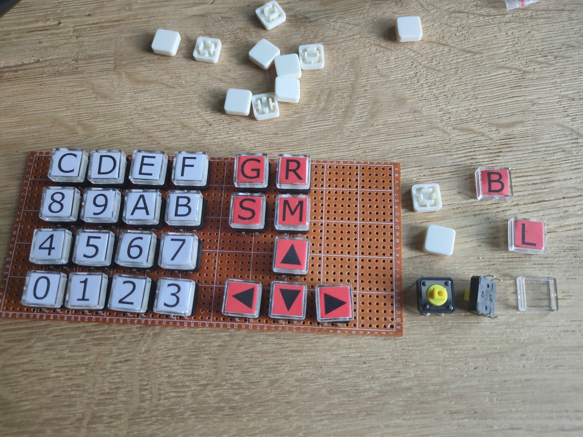
- Mini matrix keyboard removed, and used the temporary cursor buttons for the test with a rom which allows for a 8bits upload method using a arduino and the 6522. (I’m working on the big keyboard)
Work in progress code
PORT2B = $5000 		; VIA PORTB
PORT2A = $5001 		; VIA PORTA
DDR2B = $5002  		; Data direction register
DDR2A = $5003  		; Data direction register

PORTB = $6000 		; display
PORTA = $6001 		; control display + matrix keyboard
DDRB = $6002  		; data direction register
DDRA = $6003  		; data direction register
SID = $7000   		; sid base address

E  = %10000000		; enable bit
RW = %01000000		; RW bit
RS = %00100000		; Register Select bit
HOME = %00000010 	; VIA PORTB HOME command
DADDR = %00010000 	; VIA DADDRESS

LINENO = $0200		; temp address linenumber (move to other location)
NEXTLINE = 40		; 2x16 Chars but internally 40


  .org $8000

reset:
  ldx #$ff
  txs		; reset stack

; ###################################################
; #                 DISPLAY CONTROL                 #
; ###################################################
; VIA Setup

  lda #%11111111 	; Set all pins on port B to output
  sta DDRB
  lda #%11100000 	; Set top 3 pins on port A to output
  sta DDRA

; DISPLAY Setup
  lda #%00111000 	; Set 8-bit mode; 2-line display; 5x8 font
  jsr lcd_instruction
  lda #%00001110 	; Display on; cursor on; blink off
  jsr lcd_instruction
  lda #%00000110 	; Increment and shift cursor; don't shift display
  jsr lcd_instruction
  lda #$00000001 	; Clear display
  jsr lcd_instruction

; ###################################################
; #             PRINT MESSAGE LINE NO 0             #
; ###################################################
  lda #0  		; set line number
  sta LINENO      	; store for subroutine
  jsr gotoline		; move cursor

  ldx #0		; message index pointer
print:
  lda message0,x 	; start of message
  beq nextprint      	; stop when null in message (asciiz <- Zero padded)
  jsr print_char	; print char
  inx			; incr index
  jmp print		; resume print
; ###################################################
; #             PRINT MESSAGE LINE NO 1             #
; ###################################################
nextprint:
  lda #1  		; set line number
  sta LINENO      	; store
  jsr gotoline
  ldx #0  		; index pointer
print2:
  lda message1,x  	; absolute address message + x in A
  beq sidsound        	; if x is 0, end of message
  jsr print_char  	; jump subroutine
  inx             	; increment x
  jmp print2      	; loop print2


; ###################################################
; #             SID SOUND                           #
; ###################################################
sidsound:
  lda #0
  sta SID+$5		; attack/decay duration

  lda #250
  sta SID+$6		; sustain level/release duration

  lda #$95		; frequency voice 1 low byte
  sta SID+$0

  lda #$44		; frequency voice 1 high byte
  sta SID+$1

  lda #%00100001	; sawtooth + gate
  sta SID+$4		; control register voice 1

  lda #$0f		; filter mode and volume (bits 3-0 main volume)
  sta SID+$18		; filter mode and volume


; ###################################################
; #             2ND VIA                             #
; ###################################################
  lda #%11111111 	; set port A output
  sta DDR2A

  lda #%11111111	; all ones!
  sta PORT2A
; ###################################################
  lda #%11111111 	; set port A output
  sta DDR2A

  lda #%11111111	; all ones!
  sta PORT2A


; ###################################################
; #             MAIN PROGRAM LOOP                   #
; ###################################################
loop:
  jmp loop
;                   1234567812345678
message0: .asciiz  "VIA 1,2 SID TEST"
message1: .asciiz  "   FASH  2022   "

; ###################################################
; #             ONLY SUBROUTINES                    #
; ###################################################

; ###################################################
; #             Subroutine gotoline                 #
; # Moves character placement position on display   #
; # Needs : $LINENO ADDRESS                         #
; # Exit values : -                                 #
; # Destroys registers: -                           #
; ###################################################

gotoline:
  pha                             ; store a
  txa
  pha                             ; store x
  ldx LINENO
  lda #HOME                       ; cursor down
  jsr lcd_instruction
  lda #$80
nextline:
  ldx LINENO
  cpx #00
  beq endnextlines
loopline:
  adc #40
  jsr lcd_instruction
  dex
  stx LINENO
  jmp nextline
endnextlines:
  pla                             ; pop a
  tax                             ; a to x
  pla                             ; pop a
  rts


; ###################################################
; #             LCD SUBROUTINES                     #
; ###################################################
lcd_wait:
  pha
  lda #%00000000  ; Port B is input
  sta DDRB
lcdbusy:
  lda #RW
  sta PORTA
  lda #(RW | E)
  sta PORTA
  lda PORTB
  and #%10000000
  bne lcdbusy
  lda #RW
  sta PORTA
  lda #%11111111  ; Port B is output
  sta DDRB
  pla
  rts
lcd_instruction:
  jsr lcd_wait
  sta PORTB
  lda #0         ; Clear RS/RW/E bits
  sta PORTA
  lda #E         ; Set E bit to send instruction
  sta PORTA
  lda #0         ; Clear RS/RW/E bits
  sta PORTA
  rts
print_char:
  jsr lcd_wait
  sta PORTB
  lda #RS         ; Set RS; Clear RW/E bits
  sta PORTA
  lda #(RS | E)   ; Set E bit to send instruction
  sta PORTA
  lda #RS         ; Clear E bits
  sta PORTA
  rts

nmi:
  rti

irq:
  rti

  .org $fffa
  .word nmi
  .word reset
  .word irq
;  .word $0000