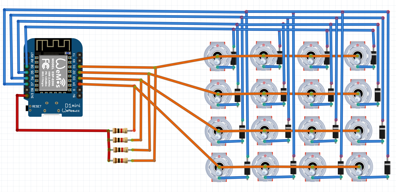
I wrote a python script to generate binary data to include in my Arduino sketch.
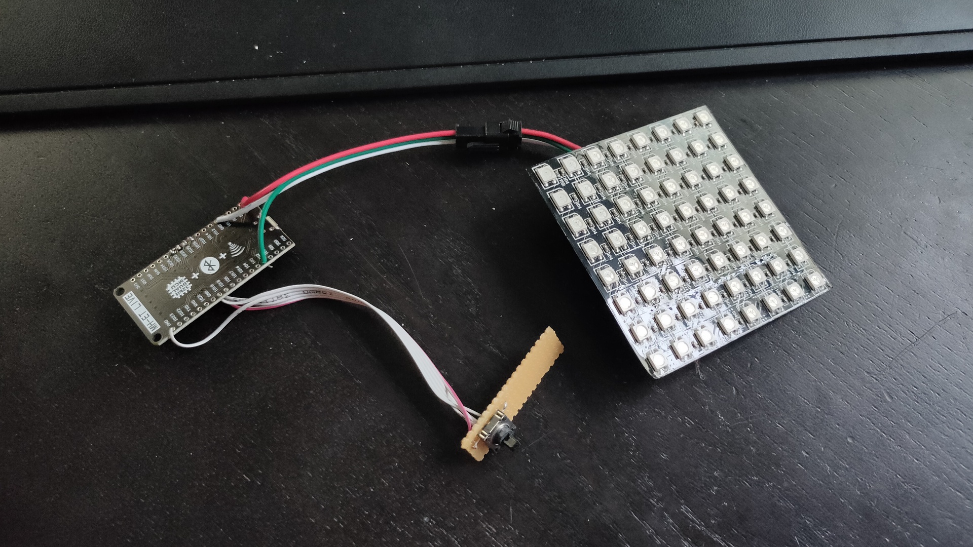
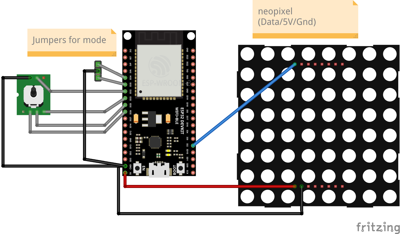
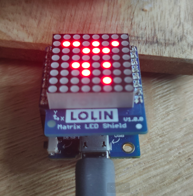
This Arduino displays codes send though MQTT.
https://en.wikipedia.org/wiki/Baudot_code
CODE:
python3 matrix.py apple gives me
byte apple_Char[8] = {
  0b00000000,
  0b01000100,
  0b01111000,
  0b00000000,
  0b00110000,
  0b00000000,
  0b00111000,
  0b00000000
};

Python Code
import sys

a = [
        [0,0,0,0,0,0,0,0 ],
        [0,0,0,0,0,0,0,0 ],
        [0,0,0,0,0,0,0,0 ],
        [0,0,0,0,0,0,0,0 ],
        [0,0,0,0,0,0,0,0 ],
        [0,0,0,0,0,0,0,0 ],
        [0,0,0,0,0,0,0,0 ],
        [0,0,0,0,0,0,0,0 ]
    ]

letters = [
        [0,1,1,0,0,0,0,0 ],
        [0,1,0,0,0,1,1,0 ],
        [0,0,1,0,1,1,0,0 ],
        [0,1,0,0,0,1,0,0 ],
        [0,1,0,0,0,0,0,0 ],
        [0,1,0,0,1,1,0,0 ],
        [0,0,1,0,0,1,1,0 ],
        [0,0,0,0,1,0,1,0 ],
        [0,0,1,0,1,0,0,0 ],
        [0,1,1,0,0,1,0,0 ],
        [0,1,1,0,1,1,0,0 ],
        [0,0,1,0,0,0,1,0 ],
        [0,0,0,0,1,1,1,0 ],
        [0,0,0,0,1,1,0,0 ],
        [0,0,0,0,0,1,1,0 ],
        [0,0,1,0,1,0,1,0 ],
        [0,1,1,0,1,0,1,0 ],
        [0,0,1,0,0,1,0,0 ],
        [0,1,0,0,1,0,0,0 ],
        [0,0,0,0,0,0,1,0 ],
        [0,1,1,0,1,0,0,0 ],
        [0,0,1,0,1,1,1,0 ],
        [0,1,1,0,0,0,1,0 ],
        [0,1,0,0,1,1,1,0 ],
        [0,1,0,0,1,0,1,0 ],
        [0,1,0,0,0,0,1,0 ]
        ]

number=0
word=str(sys.argv[1])

for col in range(len(word)) :
    character=word[col]

    number = ord(character) - 97
    nextcol = col + 1
    for row in range(len(a[col])) :
        a[row][nextcol] = letters[number][row]


print("byte " + word + "_Char[8] = {")
for i in range(len(a)) :
    print("  0b", end = '')
    for j in range(len(a[i])) :
        print(a[i][j], end="")
    if i < 7:
        print(",")
print()
print("};")
Arduino test code
#include <ESP8266WiFi.h>
#include <PubSubClient.h>
#include <WiFiClient.h>


#include "WEMOS_Matrix_LED.h"
MLED mled(5); //set intensity=5

const char* wifi_ssid = "MYSSID"; // Enter your WiFi name
const char* wifi_password =  "MYSSIDPASS"; // Enter WiFi password
const char* mqtt_server = "MYMQTTSERVER";
const int mqtt_port = 1883;
const char* mqttUser = "";
const char* mqttPassword = "";
#define MSG_BUFFER_SIZE  (50)
char msg[MSG_BUFFER_SIZE];
int value = 0;

WiFiClient espClient;

PubSubClient mqtt(espClient);

void setup_wifi() {
  delay(10);
  WiFi.mode(WIFI_STA);
  WiFi.begin(wifi_ssid, wifi_password);
  while (WiFi.status() != WL_CONNECTED) {
    delay(500);
  }
}

byte clear_Char[8] = {
  0b00000000,
  0b00000000,
  0b00000000,
  0b00000000,
  0b00000000,
  0b00000000,
  0b00000000,
  0b00000000
};

byte baudot_Char[8] = {
  0b11111111,
  0b01101010,
  0b00011100,
  0b11111111,
  0b00110100,
  0b00010000,
  0b00000100,
  0b11111111
};


#define TIME 500

void setup() {
    Serial.begin(115200);
      setup_wifi();
        mqtt.setServer(mqtt_server, mqtt_port);

WiFiClient espClient;
PubSubClient mqtt(espClient);

  mqtt.setClient(espClient);
  mqtt.setServer(mqtt_server, mqtt_port);
      delay(500);

  mqtt.subscribe("escape/matrixledin");
        delay(500);

  mqtt.setCallback(callback);

  }

void callback(char* topic, byte* payload, unsigned int length) {
        Serial.println("callback");
    String topicStr = topic;
      byte value = atoi((char*)payload);
        snprintf (msg, MSG_BUFFER_SIZE, "%1d", value);

              mqtt.publish("escape/matrixledout", msg);
       if (value == 1){

drawChar(baudot_Char);

 }else if (value == 0){
  drawChar(cleat_Char);
  }else if (value == 2){
  drawChar(test_Char);
  }else if (value == 3){
  drawChar(no_Char);
 }
 }

void reconnect() {

  while (!mqtt.connected()) {
    String clientId = "matrixClient-";
    clientId += String(random(0xffff), HEX);
    if (mqtt.connect(clientId.c_str())) {
      mqtt.publish("escape/outTopic", "hello from 8x8led module");
                Serial.println("resubscribe");

      mqtt.subscribe("escape/matrixledin");
        mqtt.setCallback(callback);

    } else {
      // Wait 5 seconds before retrying
      delay(5000);
    }
  }
}

void loop() {

 if (!mqtt.connected()) {
          Serial.println("reconnect called");
    reconnect();
  }
    mqtt.loop();

}

void drawChar(byte character[8]) {
  for(int y=7;y>=0;y--) {
  for (int x=0; x <= 7; x++) {
    if (character[(7-y)] & (B10000000 >> x)) {
     mled.dot(x,y); // draw dot
    } else {
     mled.dot(x,y,0);//clear dot
    }
  }
  mled.display();
  }
}