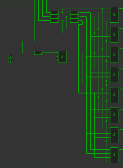
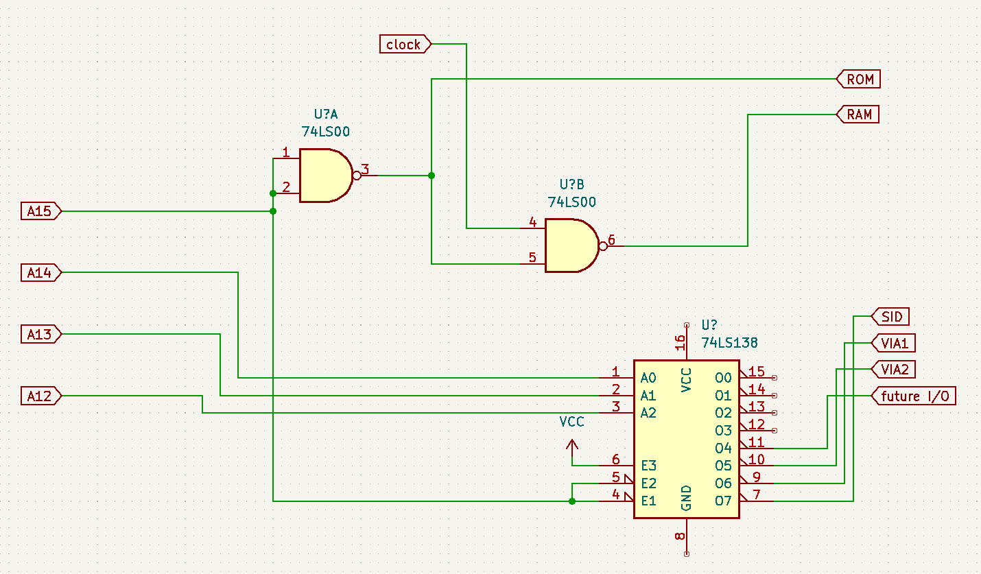
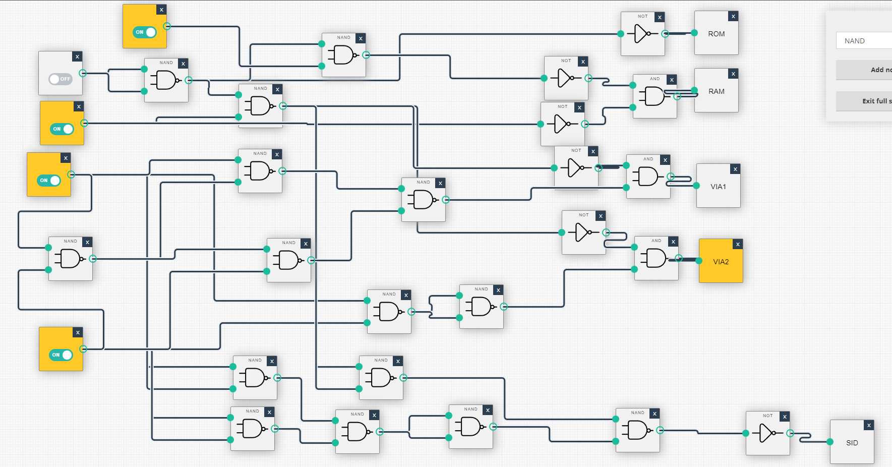
Made a simulation of my new address decoder. It uses a 74LS138 and a bunch of NAND gates. You can safe using 4 NAND gates if you are not going to use split IO
Address
8000-FFFF
ROM
ROM
7000-7FFF
Sound chip
SID
6000-6FFF
Display + cursor
VIA1
5000-5FFF
Keymatrix
VIA2
4800-4FFF
split io
IO
4000-47FF
split io
IO – ACIA
0000-3FFF
Uses clock
RAM
Above part is a single chip 74LS138
UPDATE: Found some 74LS139, so i could have changed some things around.
I found some stuff while sorting out some old computer stuff. Way back, when my Amiga was my main computer, i wanted to make my own version. A modular one.
So i started to segmentize the amiga, to put it on several exchangeable cards.
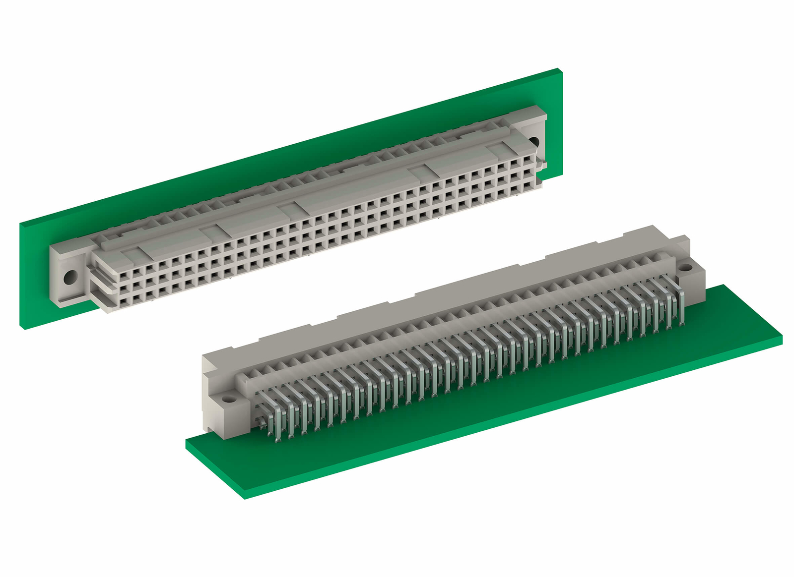
Eurocards are standardized prints 150mm x 100mm, mostly with a DIN41612 connector.
DIN41612
Eurocard example
When you make modules you can change/upgrade/test, you can have a very easy interchangeable system using a backplane like this
So i started planning those modules:
CPU – 68000 but upgradeable to 68030 or alike
Memory – With expansion
Sound
Video
More IO possibilities
Keyboard (see more at the bottom of this page)
I had a nice case which could hold a big backplane, custom powersupply. And a front panel containing drives, leds and knobs. (I know i have more info on this somewhere on my fileserver)
A nice example picture i found on danceswithferrets website
I never finished this project. I used Tech Manuals and print layouts to understand how things where done.
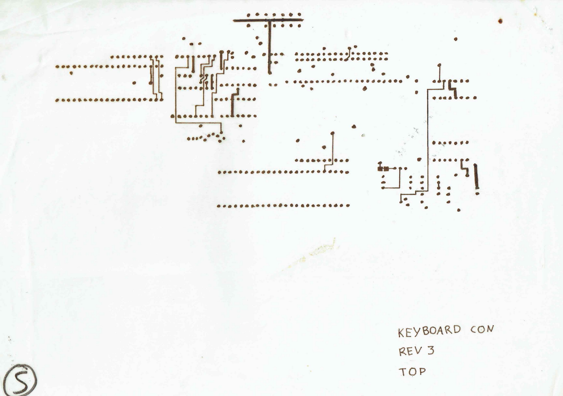
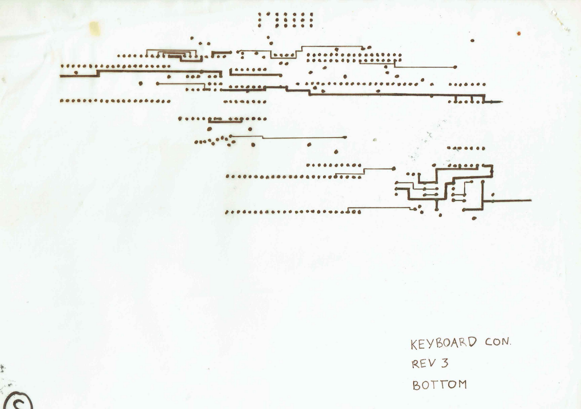
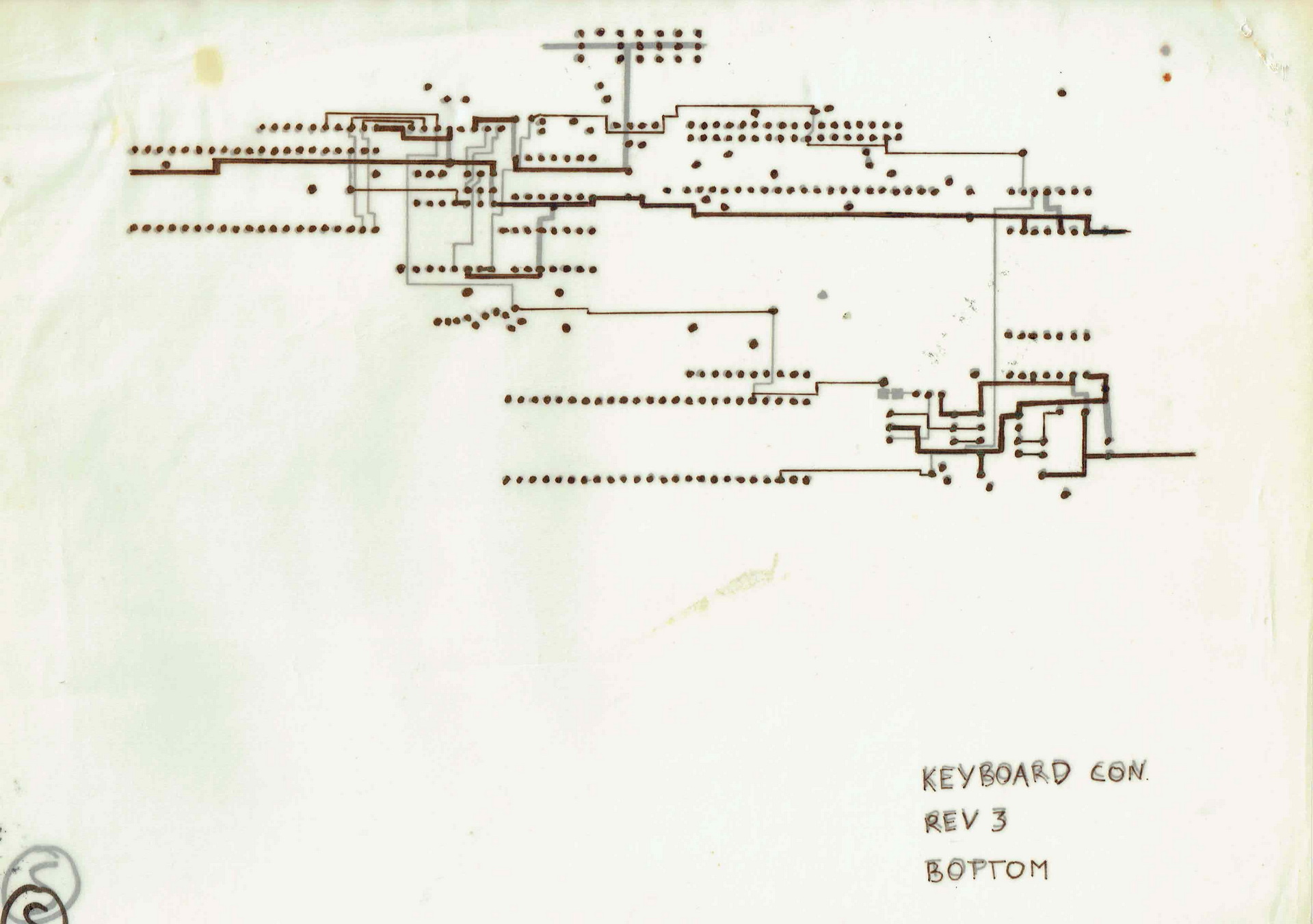
Part of schematic
I started to draw the modules like they where placed on the print on semi transparent (chalk)paper, the kind of paper that was used for electronic and mechanic diagrams.
TOP Part of printBottom part of printBoth on top of eachother
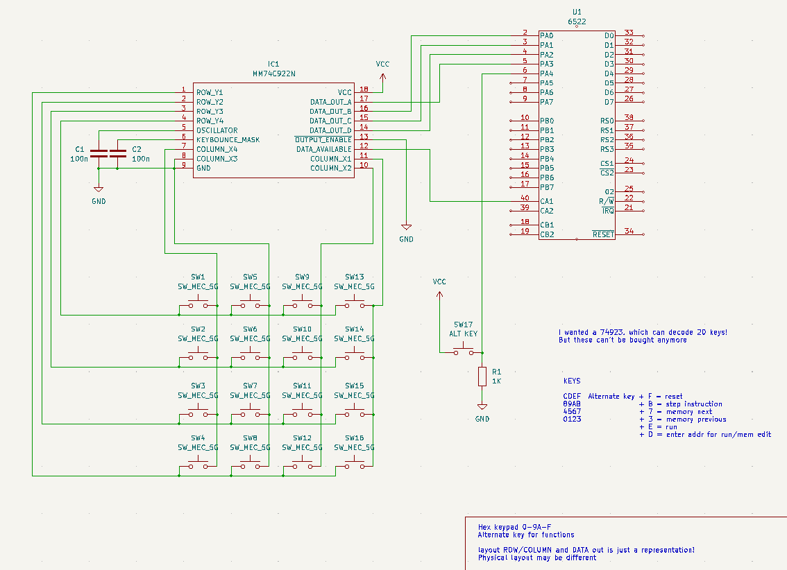
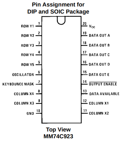
Above is my design for a hex keyboard to enter opcodes in hex using a simple monitor program. i used a 74ls922 which can decode a 4×4 matrix. I’d rather had a 74ls723 which can encode 20 keys.
Nowhere to be found. So i have to think of a new plan.
Now it is configured as follows:
C
D
E
F
8
9
A
B
4
5
6
7
0
1
2
3
When pressing the alternate key
addr (to implement)
run (1/2 implemented)
reset (to implement)
step instruction (to implement)
memory next
memory previous
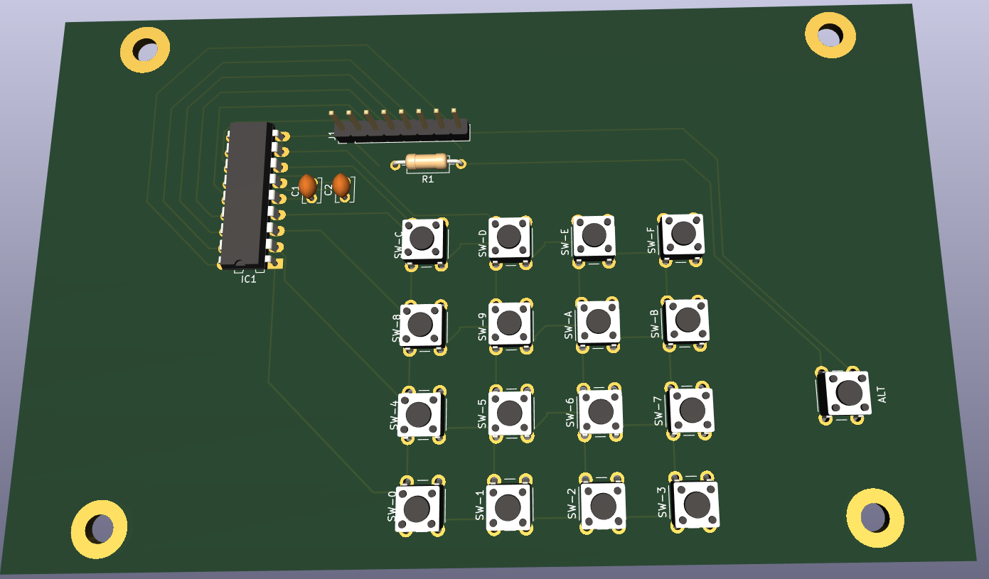
PCB design for matrix hexboard with place for notes
Meanwhile i’ve ordered new keys (the ones i’ve been using for my photomanager project and wnat to have a setup like this:
?
?
addr
run
reset
C
D
E
F
?
8
9
A
B
step
4
5
6
7
mem next
0
1
2
3
mem prev
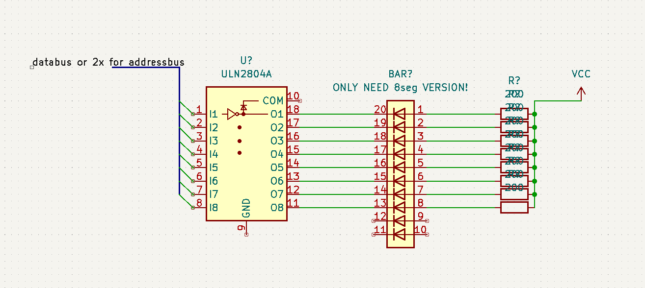
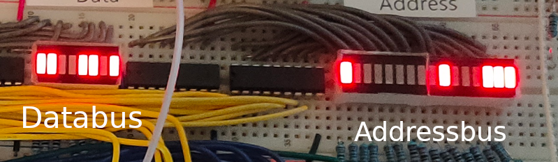
When you want to show the status of busses and alike, you can’t use a led and restistor directly on the bus, it will require too much current. So i’ve been using below schematic which uses a darlington array.
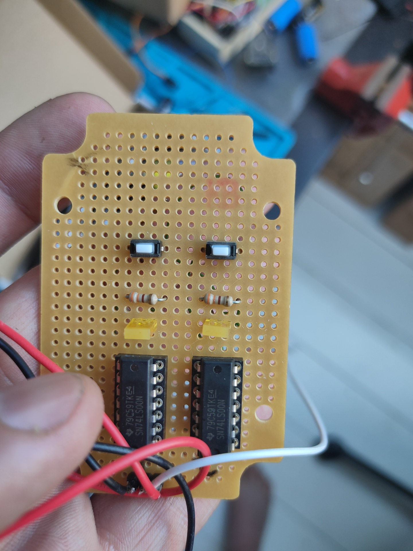
Now i can display databus, address bus and i’ve been using this for address decoding logic and hex keyboard.
I’ve implemented a second VIA chip, and ordered components to amplify the SID sound part
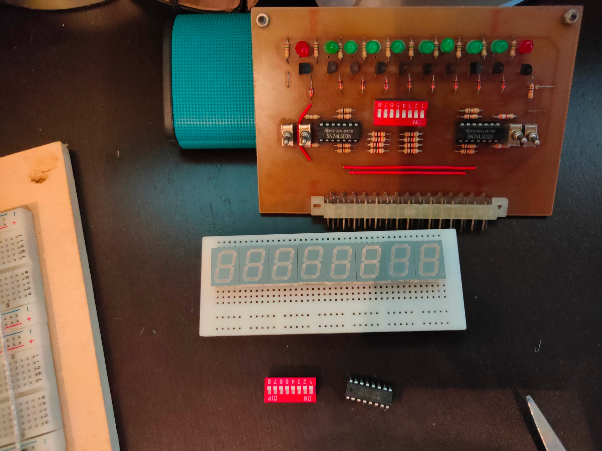
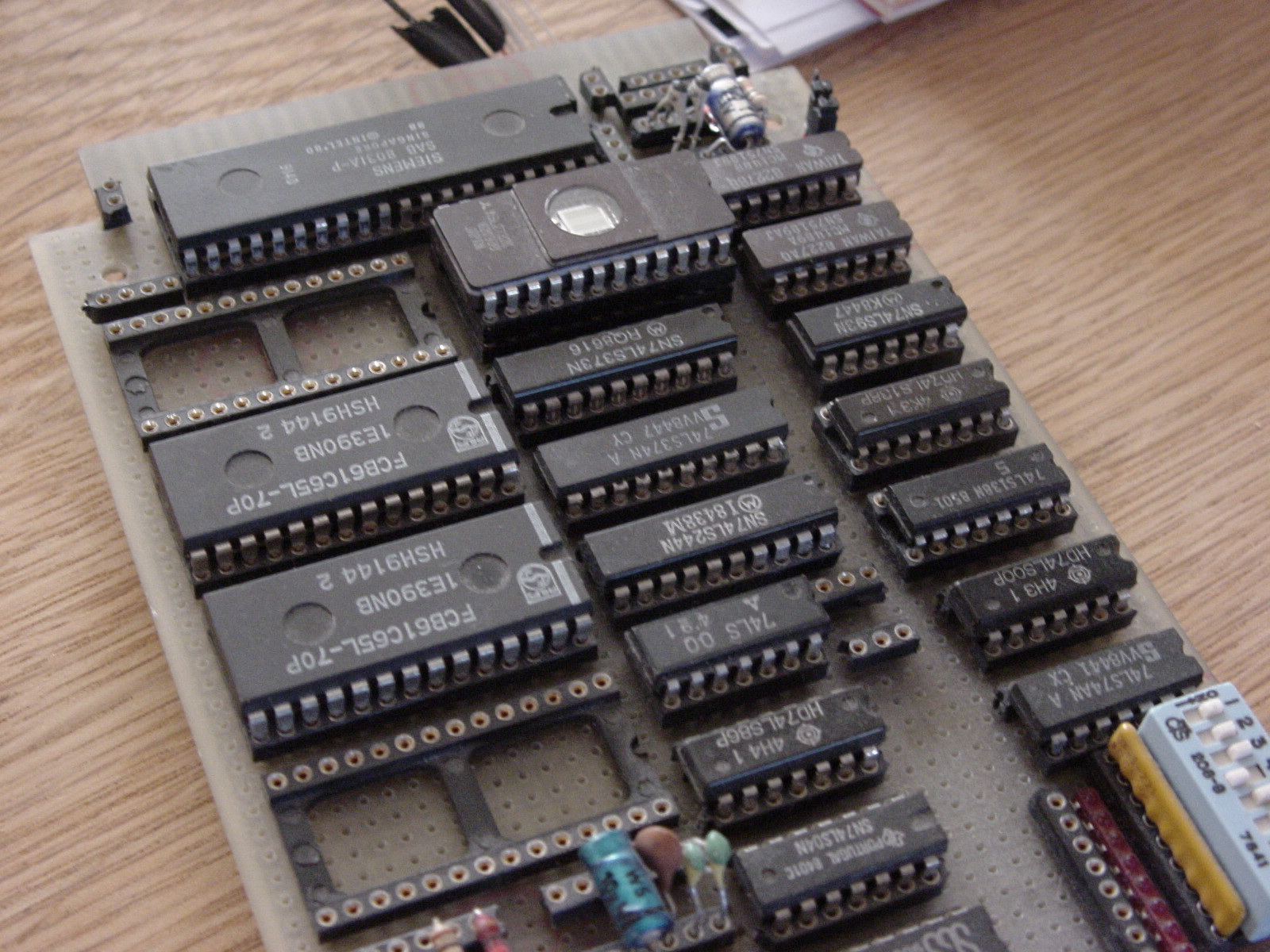
Above is my Kicad design (reverse engineering print below, which was made for my 6802CPU, which i could use to test the 6822 PIA) The 6822 is simular to 6502 in design. So i’m going to redo this for my 6502. The 7 segment displays are a start of hex-keyboard/display combo i’m going to post more of in the next days.
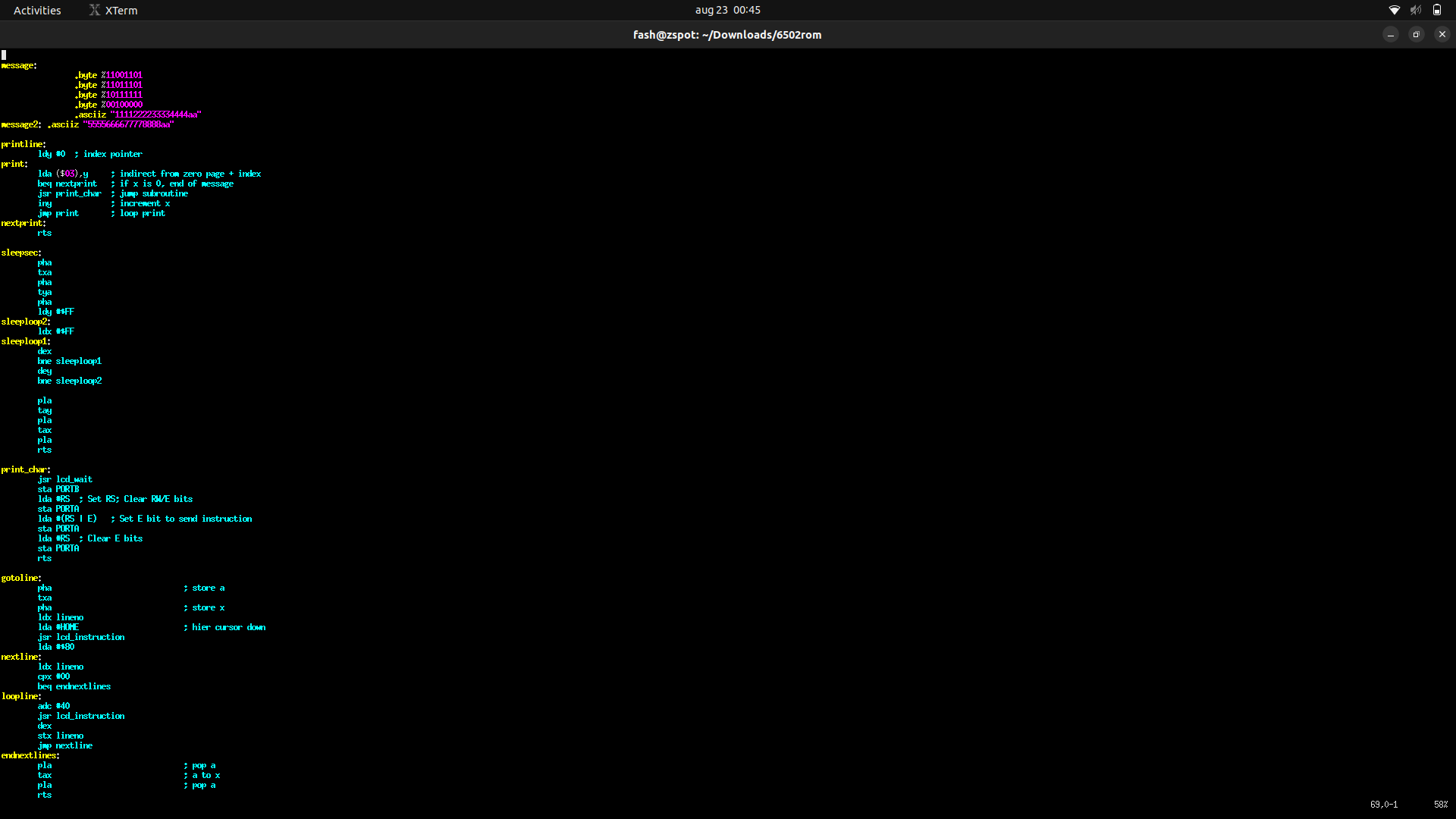
Below a part of the rom for the LCD dual line display.
Part of the ROM assembly code, top part is text (o.a. japanese)
Started to write routines which i can call to manipulate the display. Setting the pointer to a message, setting the line to use and a subset of controlls like: Center, Right, binary to ascii, scrolling, etcetera
        lda #0             ; set line number
        sta lineno         ; store
        jsr gotoline       ; goto line in display
        lda #<message      ; get address from message and store for printline subroutine
        sta messagestore
        lda #>message
        sta messagestore+1
        jsr printline      ; print

        lda #1  ; set line number
        sta lineno      ; store
        jsr gotoline
        lda #<message2
        sta messagestore
        lda #>message2
        sta messagestore+1
        jsr printline
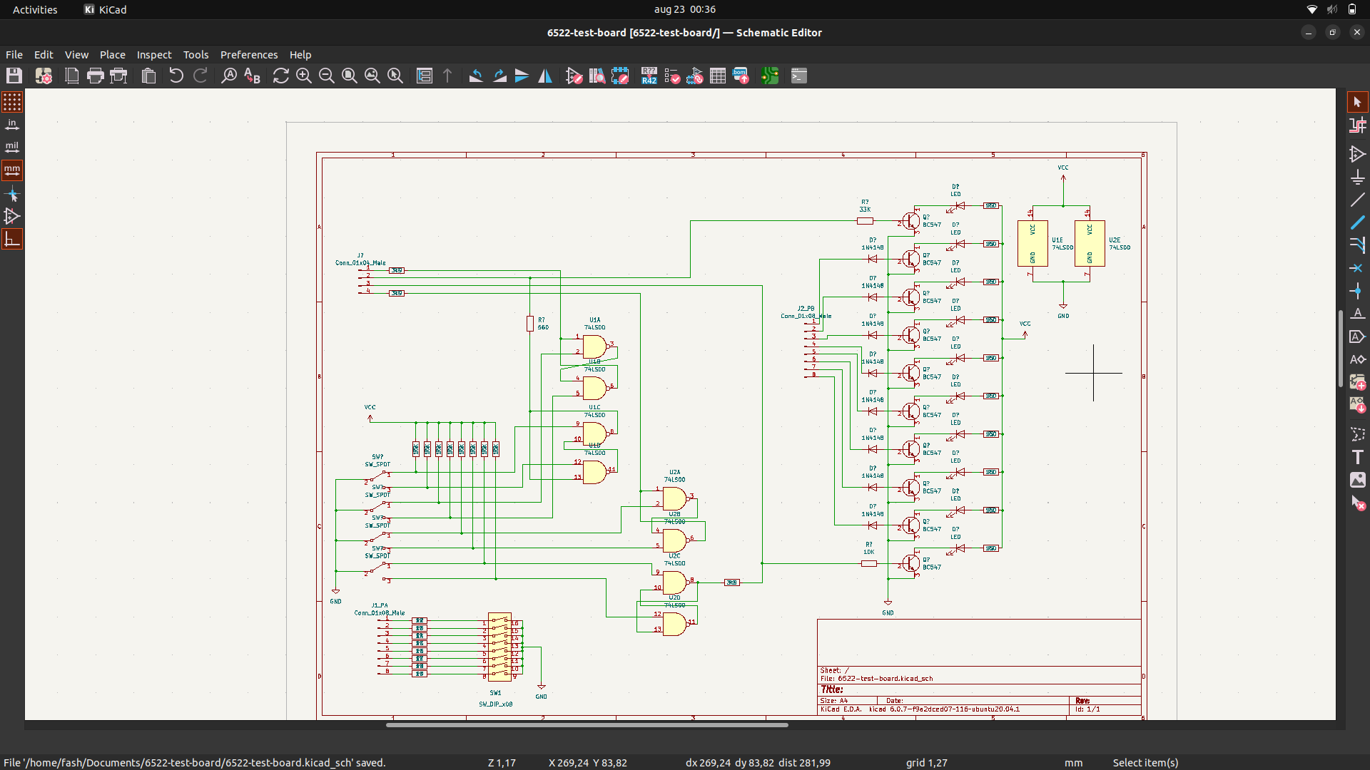
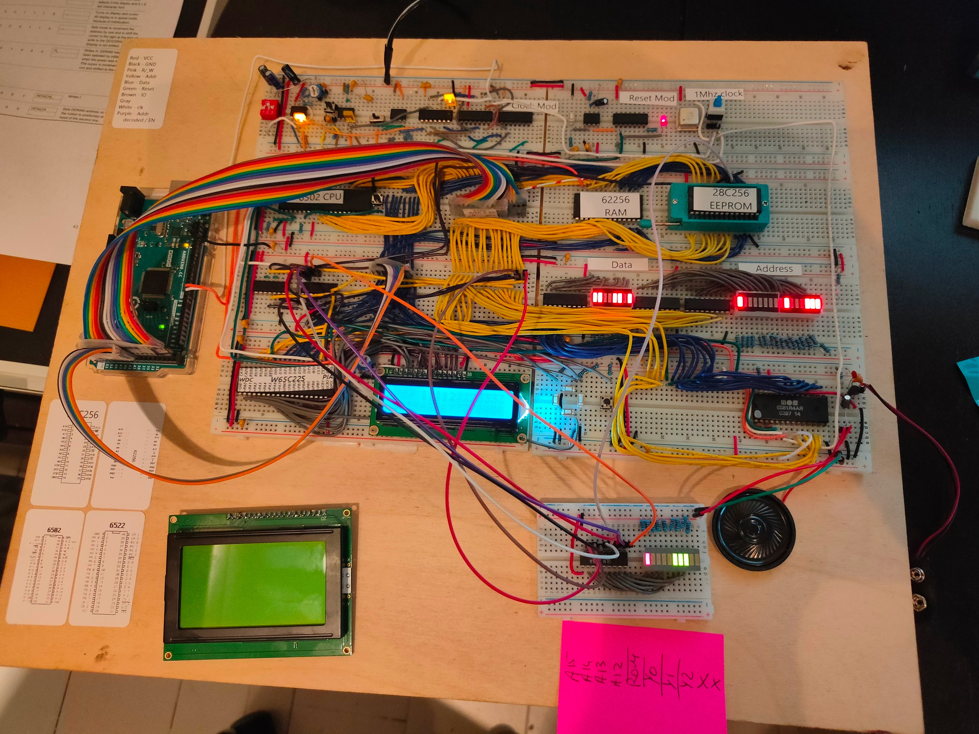
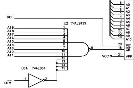
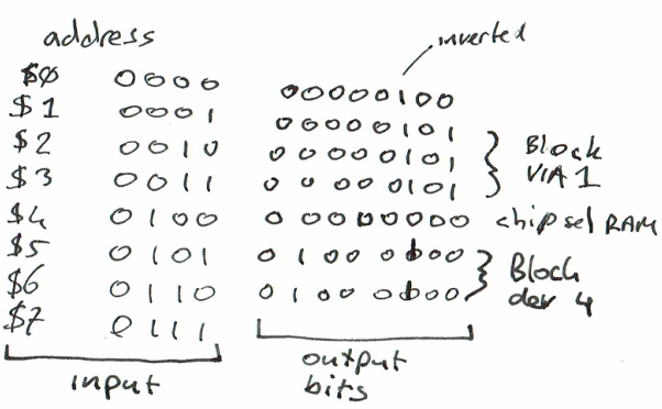
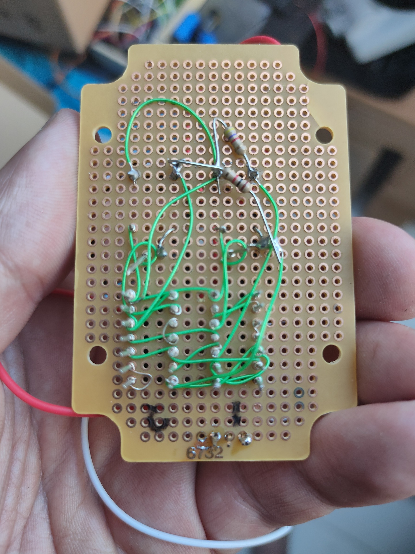
Above additions: New address decoder Below left the new graphical display, below right a test board which shows address lines and decoded chip-enable lines.
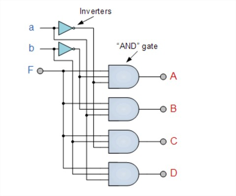
A15 high -> ROM A15 && A14 low -> RAM combination of A15 low and A14 high – A13 and A12 wil select peripherals.
Adress decoding
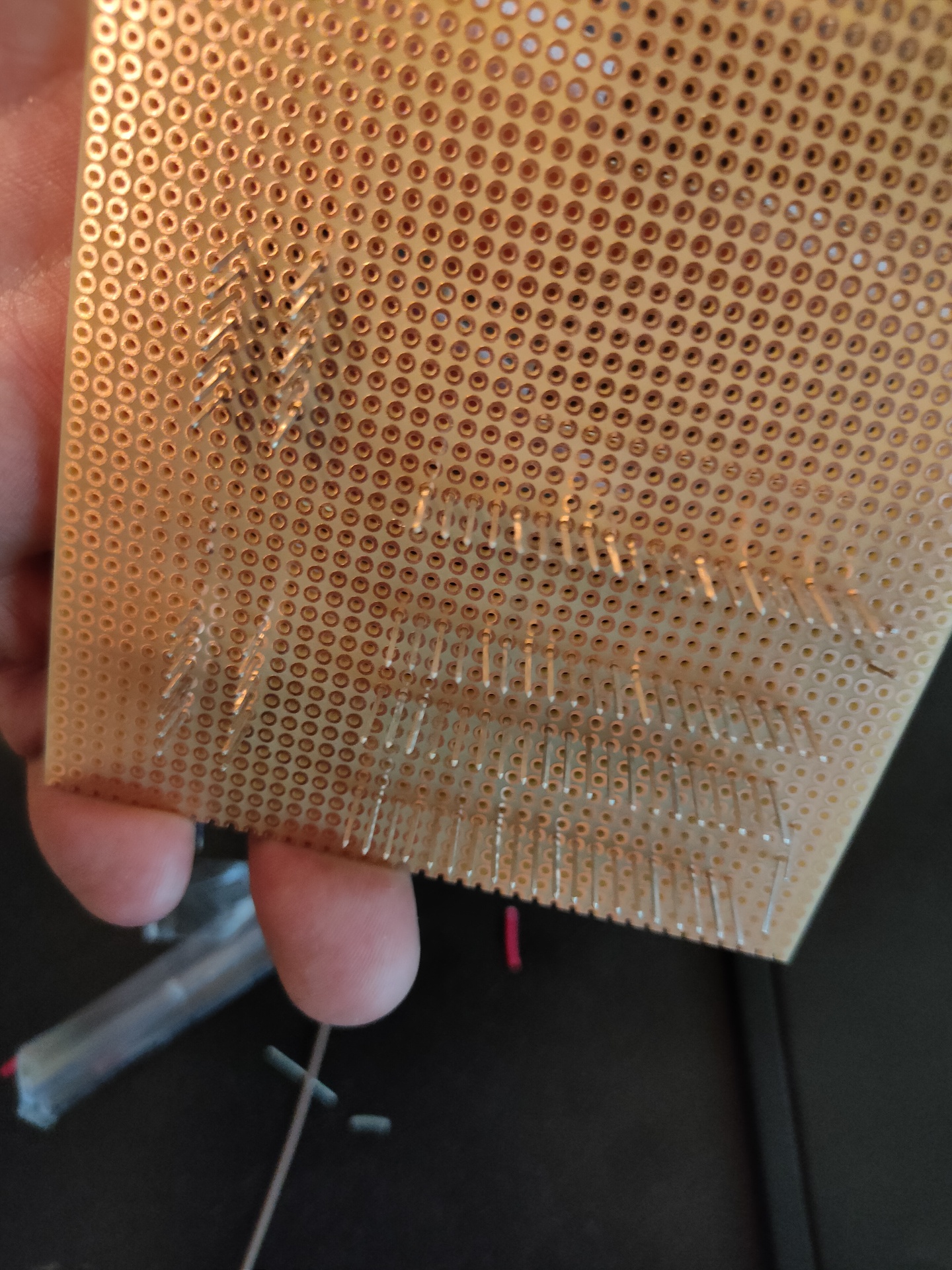
Start of a wirewrapped version
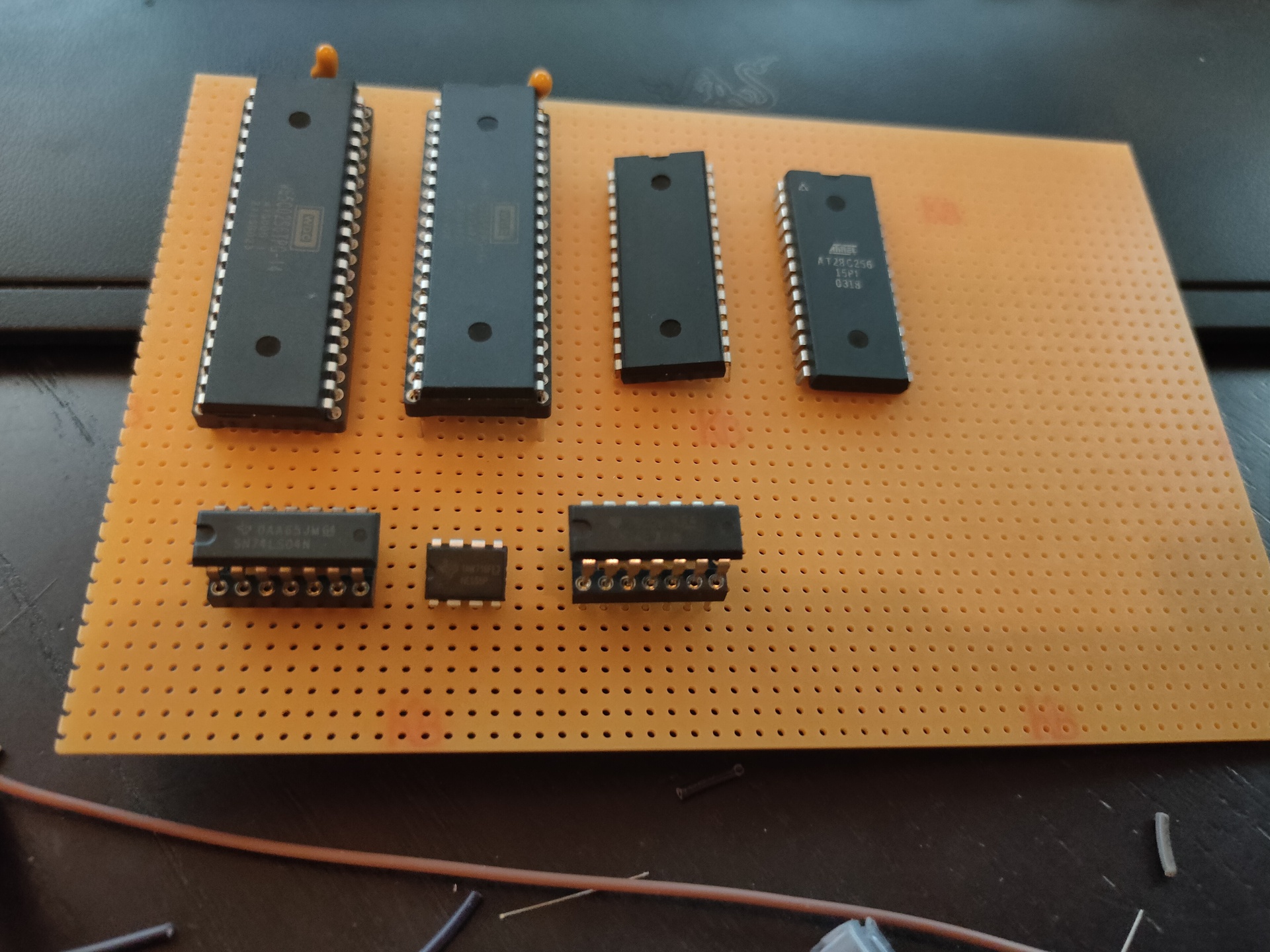
Above is a start of a wirewrapped version, i also started a PCB design in KIcad that will continuously be changed as i alter designs.
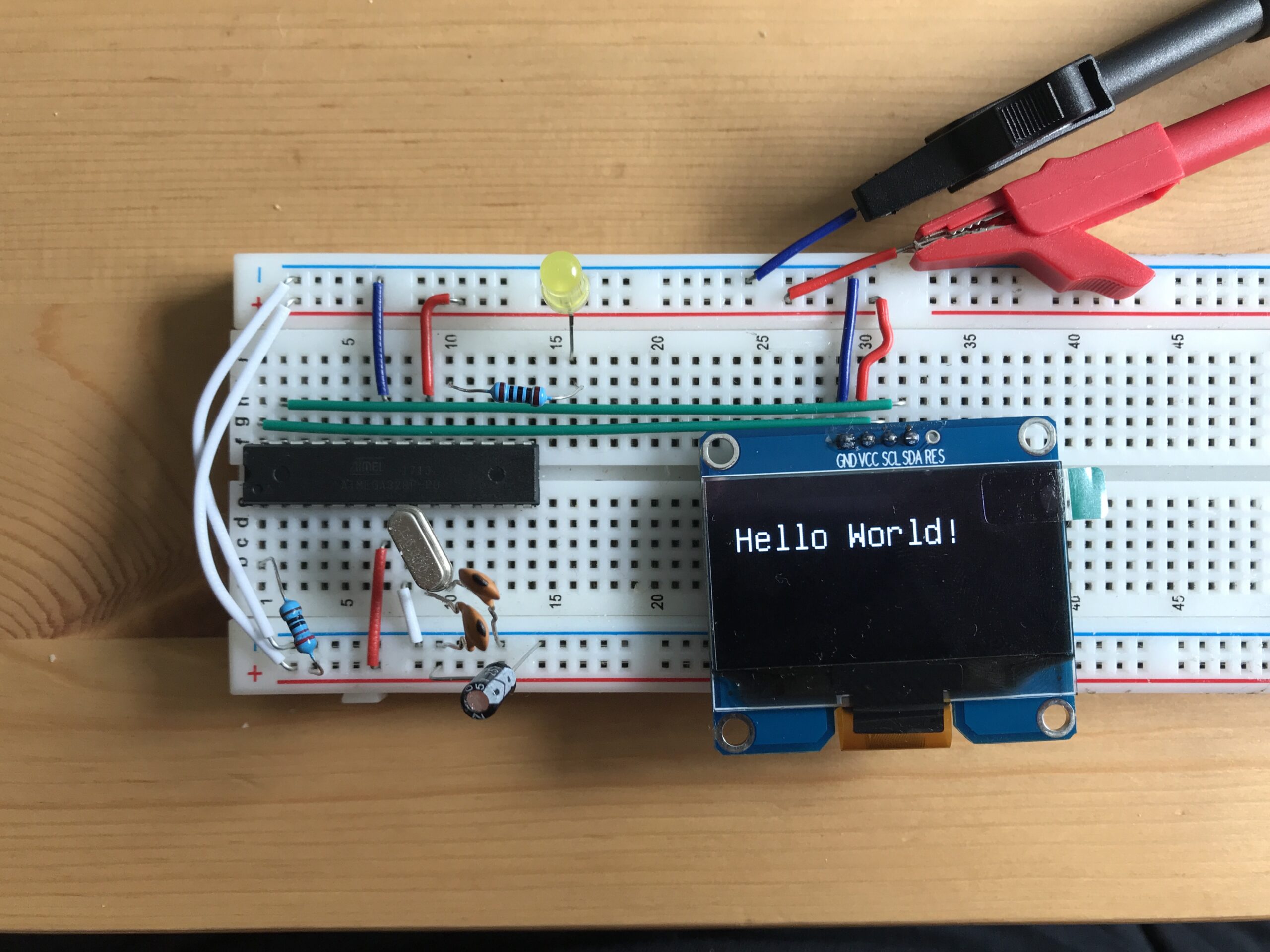
UPDATE SID Working! Using new address decoder.
SID = $7000

makesound:
	lda #0
	sta SID+$5 ; Channel1 - attack/decay

	lda #250
	sta SID+$6 ; Channel1 - Sustain/Release

	lda #$95
	sta SID+$0 ; Channel1 - Frequency low-byte

	lda #$44
	sta SID+$1 ; Channel1 - Frequency high-byte

	lda #%00100001
	sta SID+$4 ; SAW + Gate

	lda #$0f
	sta SID+$18 ; Volume max
For accessing the different components in computers you have to use the Address Bus. In most 8 bits computers there are 16 address lines.
The CPU on a 6502 can access 65536 addresses (16 bit ). But most chips in the circuit have just a few address lines. So the chip to use has to be selected using a CE (chip Enable) signal.
Old article i found on my fileserver from 1984
74 Series logic
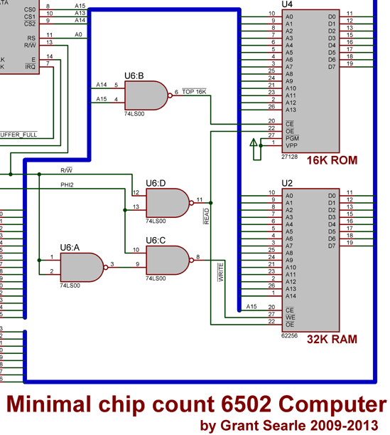
Above example uses A15 combined with A14 to address the 16K ROM When using a 32k rom in the upper part of the memory, a15 can be used as CE
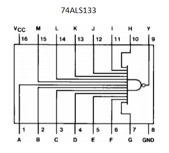
The 74ALS133 is a widely used decoder due to it’s many inputs.
Sometimes not all address lines are used for decoding, then you will get a repetition of the device in the memory map.
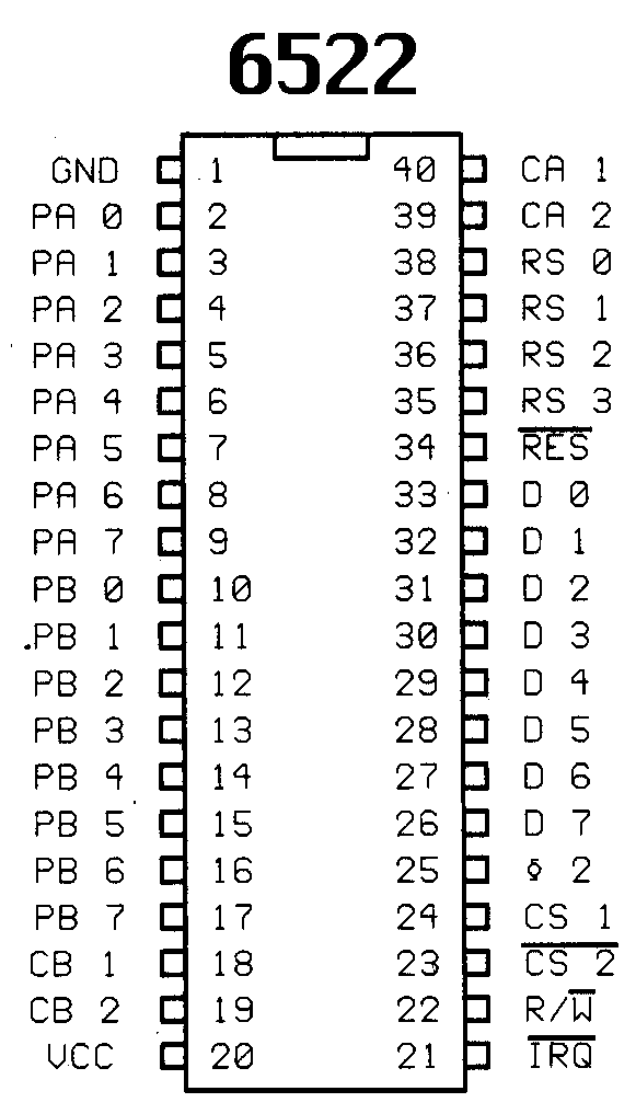
Above 6522 VIA has only 4 address lines RS0-RS3. But 2 chipselect pins (CS). If you connect the chip as below.
The chip would be selected when A15 is 1 and A14 is 0, A13-A04 it would not listen to. So its 4 bits addresses (total 16), would be repeated in a block $8000-$BFFF (10xx xxxx xxxx aaaa) 16384 addresses for 16 addresses on the 6522
ROM
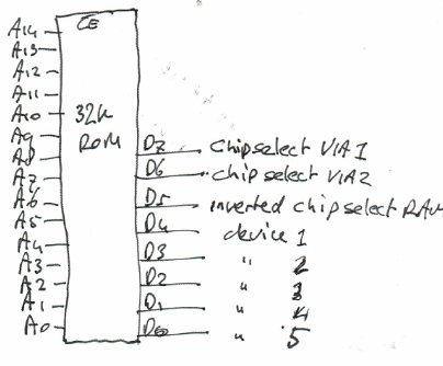
Another simple solution to get a more precise address decoder without using a lot of components is using a ROM. But this wil only work for low speeds! A eeprom is relative cheap
Example ROM as chip enable/select
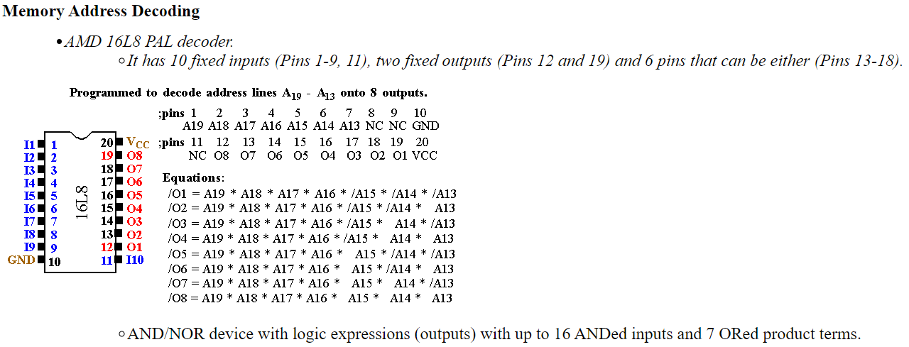
PAL PLA GAL
With these devices you can “program” a schematic which works as above example’s of the 74 series. But now you can do it using only one component.
PALs and PLAs are fuse-programmed, some are erasable like (e)eprom. Below a example of the code. Most of the PAL/PLA/GAL are hard to get and obsolete
;PALASM Design Description
;---------------------------------- Declaration Segment ------------
TITLE    pRAM PC_interface Address Decoder
PATTERN  pRAM97A.pds
REVISION H
AUTHOR   Trevor Clarkson
COMPANY  EEE KCL
DATE     30/05/97

CHIP  decode  PALCE20V8

;---------------------------------- PIN Declarations ---------------
PIN  1          AEN                                   COMBINATORIAL ; INPUT
PIN  2          A9                                    COMBINATORIAL ; INPUT
PIN  3          A8                                    COMBINATORIAL ; INPUT
PIN  4          A7                                    COMBINATORIAL ; INPUT
PIN  5          A6                                    COMBINATORIAL ; INPUT
PIN  6          A5                                    COMBINATORIAL ; INPUT
PIN  7          A4                                    COMBINATORIAL ; INPUT
PIN  8          A3                                    COMBINATORIAL ; INPUT
PIN  9          A2                                    COMBINATORIAL ; INPUT
PIN  10         A1                                    COMBINATORIAL ; INPUT
PIN  11         IOW                                   COMBINATORIAL ; INPUT
PIN  12         GND
PIN  13         IOR                                   COMBINATORIAL ; INPUT
PIN  14         ACK_HALT                              COMBINATORIAL ; INPUT
PIN  15         PLS_EN                                COMBINATORIAL ; OUTPUT
PIN  16         BRDW                                  COMBINATORIAL ; OUTPUT
PIN  17         MOD_CTRL                              COMBINATORIAL ; OUTPUT
PIN  18         RAM_ACCESS                            COMBINATORIAL ; OUTPUT
PIN  19         IO_16                                 COMBINATORIAL ; OUTPUT
PIN  20         LATCH_MOD                             COMBINATORIAL ; OUTPUT
PIN  21         LATCH_ADD                             COMBINATORIAL ; OUTPUT
PIN  22         P300                                  COMBINATORIAL ; OUTPUT
PIN  23         P300IN                                COMBINATORIAL ; INPUT
PIN  24         VCC

;PC address decoding functions (not all in this PAL)
;uses latched address to provide low-order address lines to pRAM/RAM
;       A3      A2      A1      R/W     Addr    Function
;       0       0       0       R       300     MFF_0
;                               W               not used
;       0       0       1       R       302     MFF_1
;                               W               not used
;       0       1       0       R       304     MFF_2
;                               W               not used
;       0       1       1       R       306     MFF_3
;                               W               Latch Module Number
;       1       0       0       R       308     PLS_Status  (pRAM status)
;                               W               PLS_Control (pRAM control)
;       1       0       1       R       30A     Weight/Connection-
;                               W                Pointer RAM access
;       1       1       0       R       30C     not used
;                               W               Latched RAM address
;       1       1       1       R       30E     not used
;                               W               pRAM_256 module control
;
; NB. IO_16 must be tri-stated when not in use

;----------------------------------- Boolean Equation Segment ------
EQUATIONS

/P300 = A9*A8*/A7*/A6*/A5*/A4*/IOR + A9*A8*/A7*/A6*/A5*/A4*/IOW

/BRDW = /P300IN * /IOW

/PLS_EN = /P300IN*/A3*/IOR + /P300IN*A3*/A2*/A1

; MOD_CTRL is active HIGH
MOD_CTRL = ACK_HALT * /BRDW * A3 * A2 * A1 * /IOW

; RAM_ACCESS is active HIGH
RAM_ACCESS = ACK_HALT * /P300IN * A3 * /A2 * A1

IO_16 = GND
IO_16.TRST = /P300IN
; enable 16-bit transfers

; LATCH_MOD is active HIGH
LATCH_MOD = /BRDW * /A3 * A2 * A1

; LATCH_ADD is active HIGH
LATCH_ADD = /BRDW * A3 * A2 * /A1

;----------------------------------- Simulation Segment ------------
SIMULATION
TRACE_ON A9 A8 A7 A6 A5 A4 IOR /IOW /BRDW /PLS_EN MOD_CTRL RAM_ACCESS IO_16 LATCH_MOD LATCH_ADD ACK_HALT /P300 /P300IN
SETF /A9 /A8 /A7 /A6 /A5 /A4 /A3 /A2 /A1 IOR IOW /ACK_HALT /P300IN
SETF /IOW ; test P300 doesn't respond
SETF IOW /IOR ; test P300 doesn't respond
SETF IOR
SETF A9 A8 /A7 /A6 /A5 /A4 /IOR /P300IN
SETF A1
SETF A2 /A1
SETF A1 ; read mff0-3
SETF IOR /IOW ; test P300 and BRDW
SETF /A3 A2 A1 ; test Latch Module No
SETF IOW A3 A2 A1 ; MOD-CTRL not active until ACK_HALT
SETF ACK_HALT /IOW
SETF IOW /ACK_HALT
SETF A3 /A2 A1 ; check RAM_ACCESS
SETF ACK_HALT /IOW
SETF /ACK_HALT IOW
SETF ACK_HALT /IOR ; check READ and WRITE to RAM
SETF IOR P300IN
SETF /A3 A2 A1
SETF /ACK_HALT /P300IN
SETF IOW
SETF /A3 A2 A1 /IOW ; check LATCH_MOD
SETF IOW
SETF A3 A2 /A1
SETF /IOW       ; check LATCH_ADD
SETF /A3 /A2 /A1 ; shouldn't happen normally

TRACE_OFF
;-------------------------------------------------------------------
FPGA
Example FPGA code. A solution which is too fancy for my 6502.
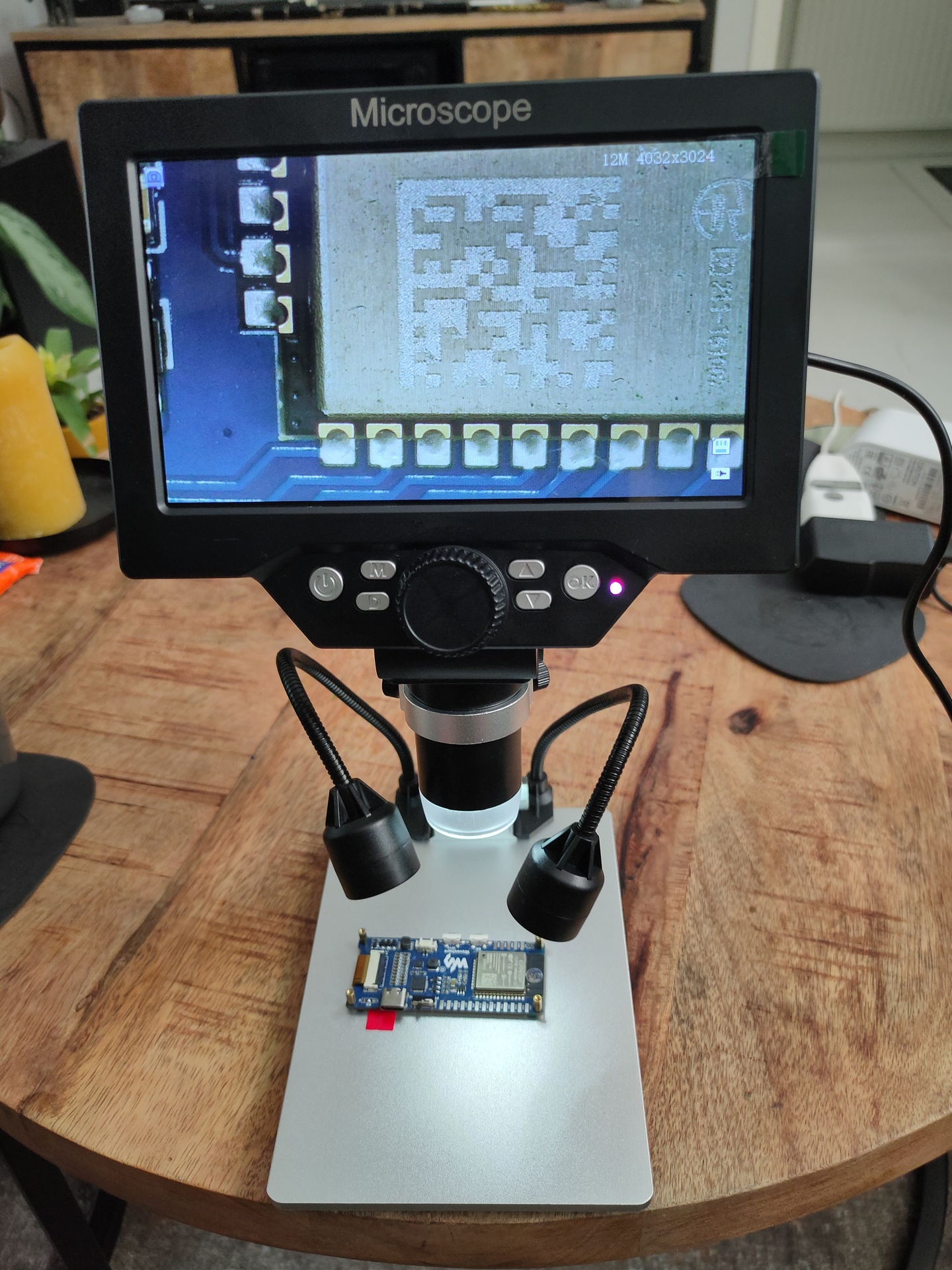
We are all getting older and electronics smaller. It’s hard to see if your soldering blobs are okay! Those blobs can reflect the light in a way that it’s not visible anymore to check them.
So i took Bigreds advice, and bought a G1200 Microscope. It’s a cheap but helpfull little gadget.
1-1200 times zoom
7inch screen (720p)
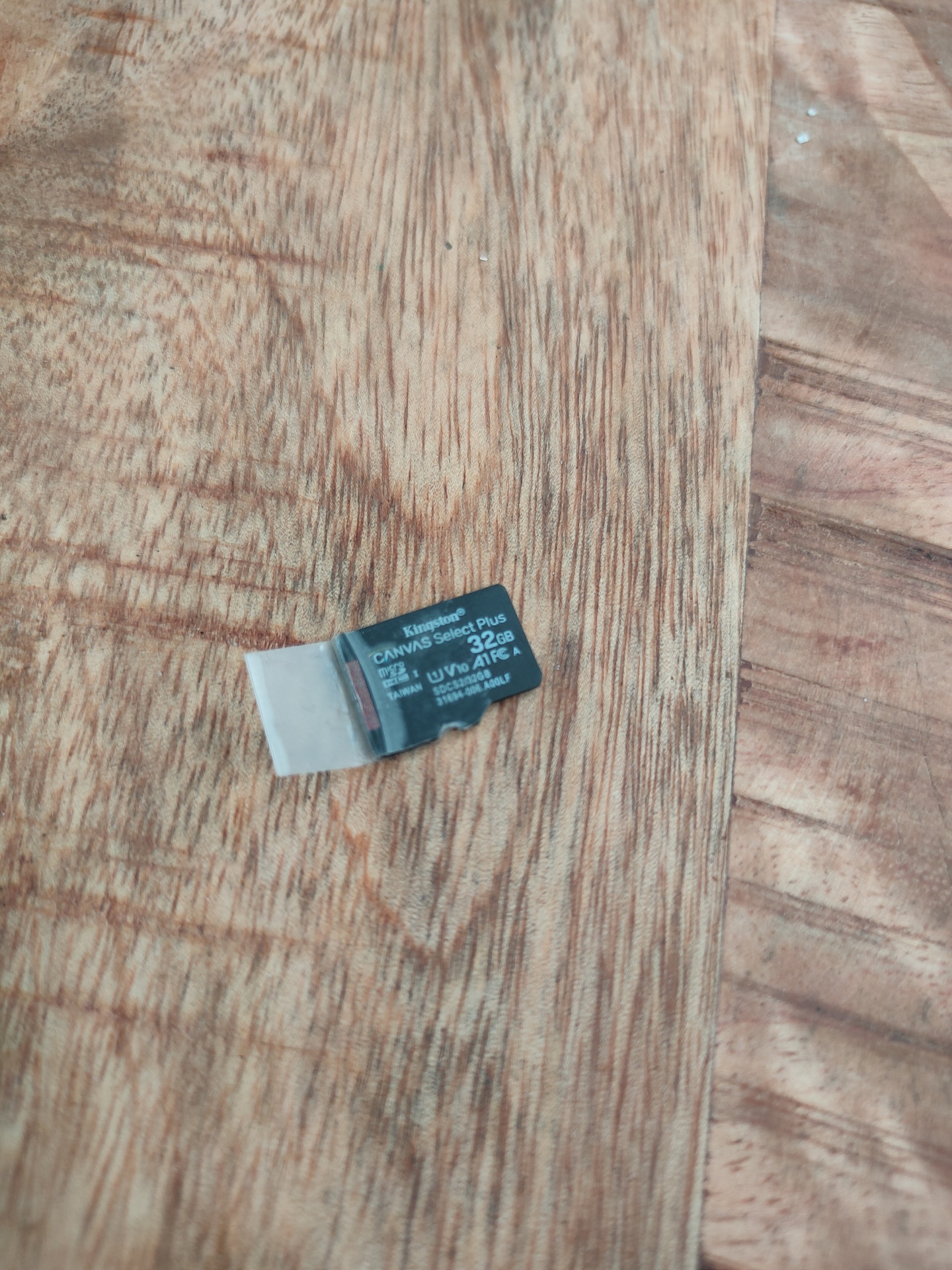
SDcard
Lipo battery
Recording on micro sdcard in 12 mega pixels pictures and 1080P Video. (even got a timer)
Focus button, and extra lights (There is a light source in de camera head, which can be adjusted by a knob)
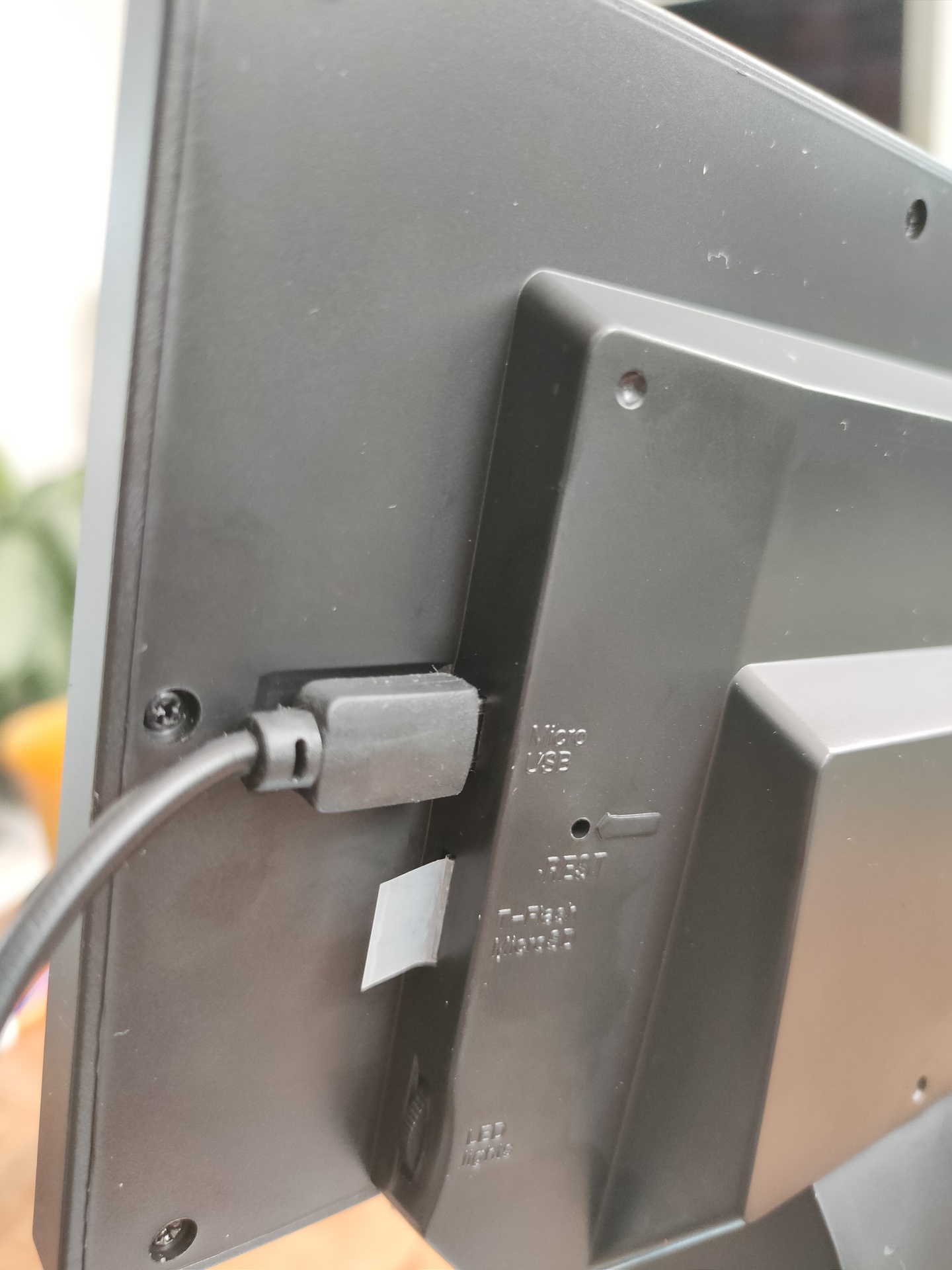
When connecting to your pc, you get 3 options
PC Camera ( … so you can record using your pc with for example OBS)
Mass Storage, to read the SDCARD
Rec_mode ?!? – No idea yet
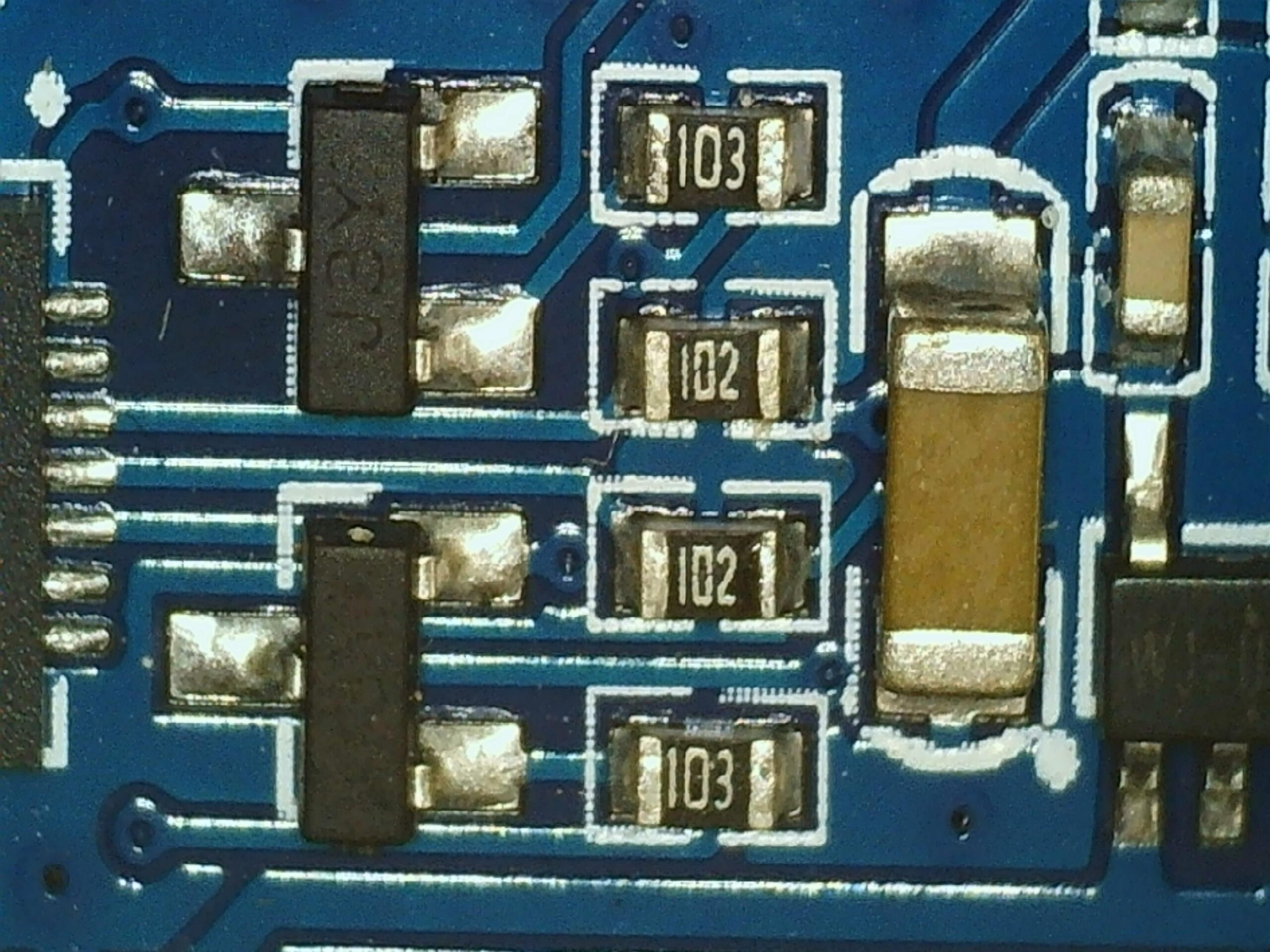
Below some examples:
Picture example
Video example
SDCard Access:
Access to the sdcard is a little hard. Connecting via Mass Storage is a solution. But i’ve put a little piece of tape to get the card in or out of the slot.
You can view the recordings on the Microscope itself. So i was wondering, can it play any other movie files?
I placed different MOV files on the sdcard, but the microscope skipped the ones i places on the sdcard myself.
I started to look at the metadata, and saw a Codec ID “qt 2016.04.21 (qt )”
 mediainfo VID_001.MOV
General
Complete name                            : VID_001.MOV
Format                                   : MPEG-4
Format profile                           : QuickTime
Codec ID                                 : qt   2016.04.21 (qt  )
File size                                : 551 MiB
Duration                                 : 12s 0ms
Overall bit rate                         : 385 Mbps
Encoded date                             : UTC 1904-01-01 00:00:00
Tagged date                              : UTC 1904-01-01 00:00:00

Video
ID                                       : 1
Format                                   : AVC
Format/Info                              : Advanced Video Codec
Format profile                           : Main@L4.1
Format settings, CABAC                   : Yes
Format settings, ReFrames                : 1 frame
Codec ID                                 : avc1
Codec ID/Info                            : Advanced Video Coding
Duration                                 : 12s 0ms
Source duration                          : 12s 360ms
Bit rate                                 : 14.5 Mbps
Width                                    : 1 920 pixels
Height                                   : 1 080 pixels
Display aspect ratio                     : 16:9
Frame rate mode                          : Constant
Frame rate                               : 25.000 fps
Color space                              : YUV
Chroma subsampling                       : 4:2:0
Bit depth                                : 8 bits
Scan type                                : Progressive
Bits/(Pixel*Frame)                       : 0.280
Stream size                              : 20.8 MiB (4%)
Source stream size                       : 21.3 MiB (4%)
Language                                 : 33
Encoded date                             : UTC 1904-01-01 00:00:00
Tagged date                              : UTC 1904-01-01 00:00:00
mdhd_Duration                            : 12000

Audio
ID                                       : 2
Format                                   : PCM
Format settings, Endianness              : Little
Format settings, Sign                    : Signed
Codec ID                                 : sowt
Duration                                 : 12s 0ms
Source duration                          : 12s 288ms
Bit rate mode                            : Constant
Bit rate                                 : 128 Kbps
Channel(s)                               : 1 channel
Channel positions                        : Front: C
Sampling rate                            : 8 000 Hz
Bit depth                                : 16 bits
Stream size                              : 188 KiB (0%)
Source stream size                       : 192 KiB (0%)
Language                                 : 33
Default                                  : Yes
Alternate group                          : 1
Encoded date                             : UTC 1904-01-01 00:00:00
Tagged date                              : UTC 1904-01-01 00:00:00
Tried to change this with ffmpeg, but it would not change the way i want.
ffmpeg -i VID_002.MOV -c copy -map 0 -brand 'qt   2016.04.21 (qt  )' VID_007.MOV

mediainfo VID_007.MOV
General
Complete name                            : VID_007.MOV
Format                                   : MPEG-4
Format profile                           : QuickTime
Codec ID                                 : qt   0000.02 (qt  )  <--------------- nope
Header of the movie clip maybe i have to look into this … later
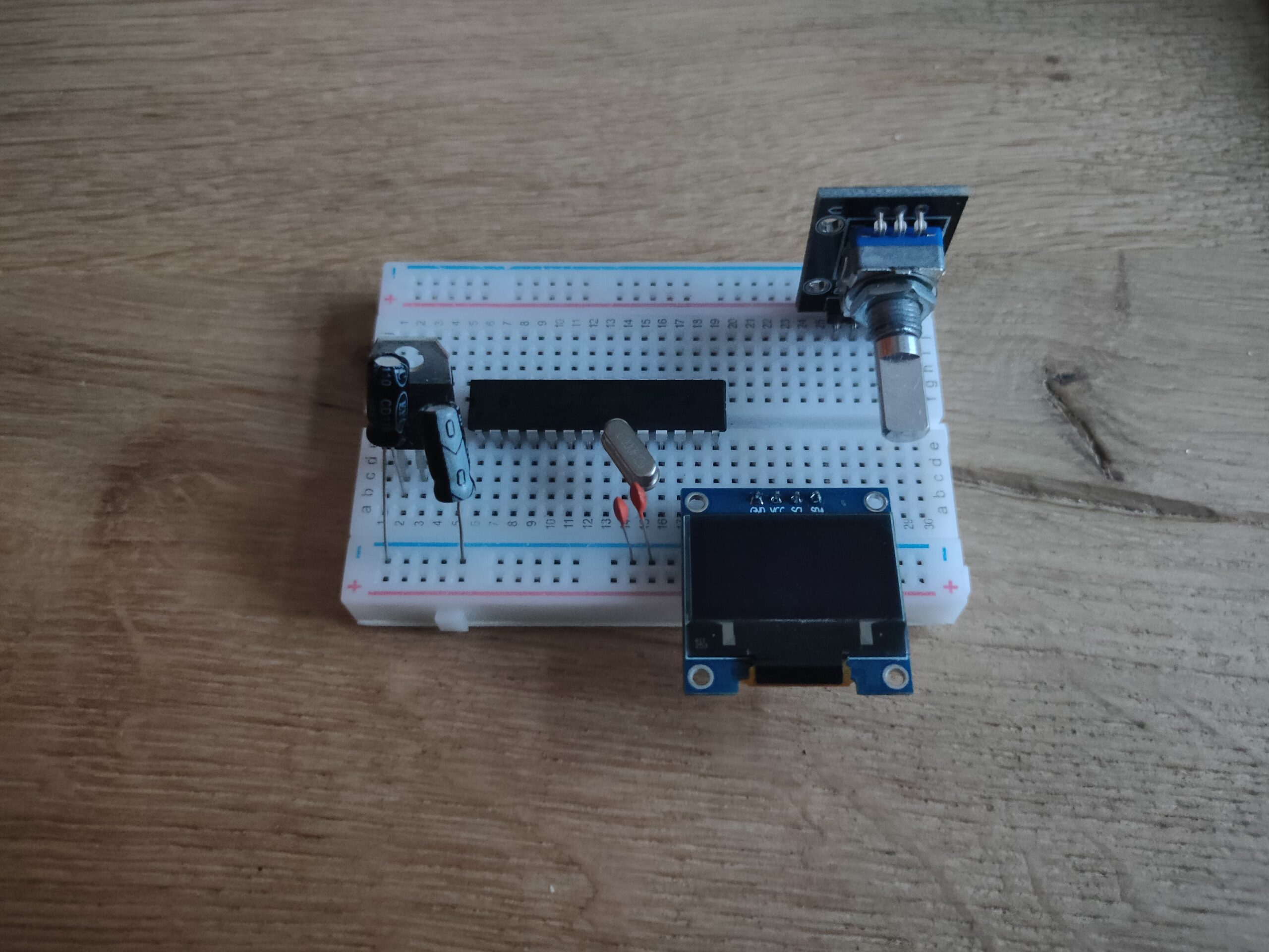
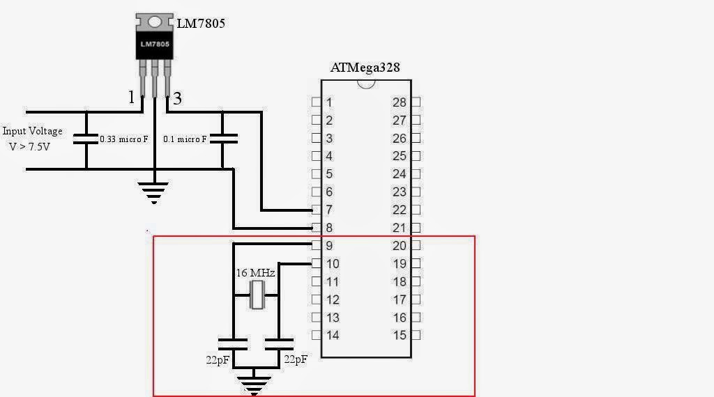
I want to make a new clock module using a bare ATmega328 running on a 16mhz crystal. This to provide a clock for my 6502 computer.
Using a display and a rotary encoder I want to create a clock module which generates a 50/50 duty cycle clock 1Hz – 1 MHz.
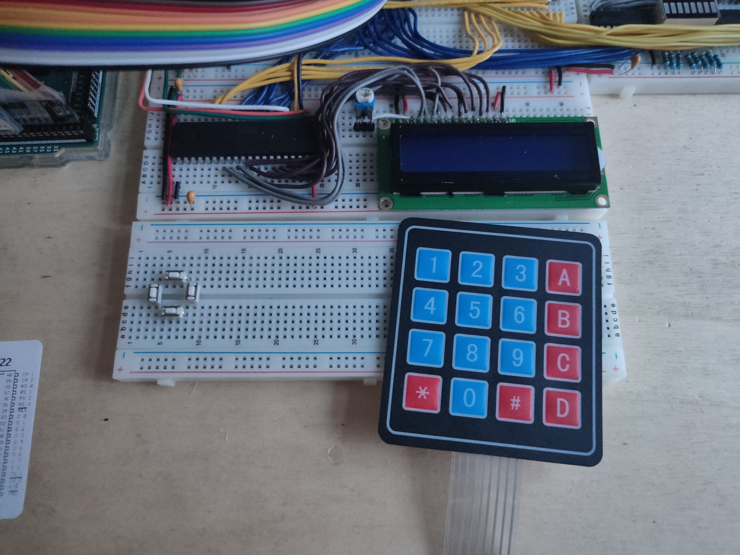
Input module for my 6502 will be 5 buttons. (For now) that’s what’s left on the VIA on port A. (Rest is used by the display). The display i’m going to place directly on the bus. But I already ordered a second VIA. Matrix keyboard will be next. Then I will use the buttons in the picture for shift/alternate buttons. Because I’ll need about 25 keys. (See other posts) . I’ll probably end up making that one myself.
I found examples like this, rest i have to think of myself
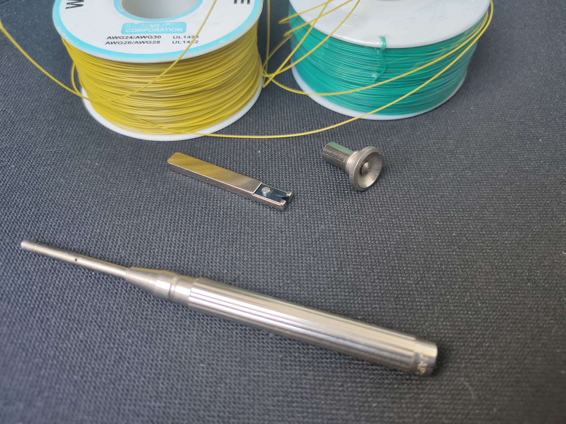
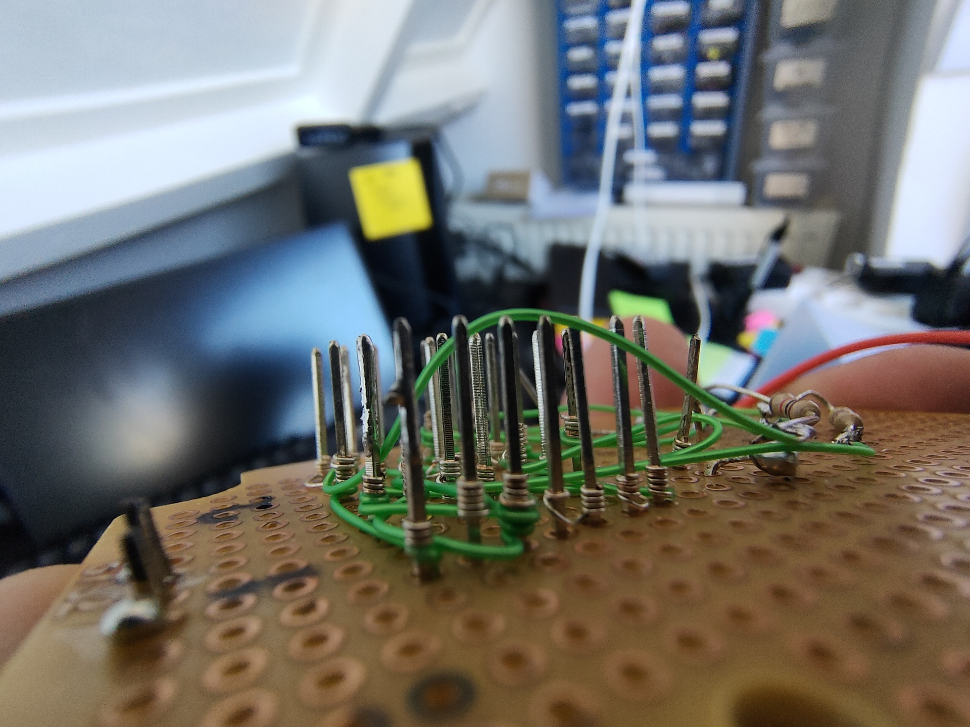
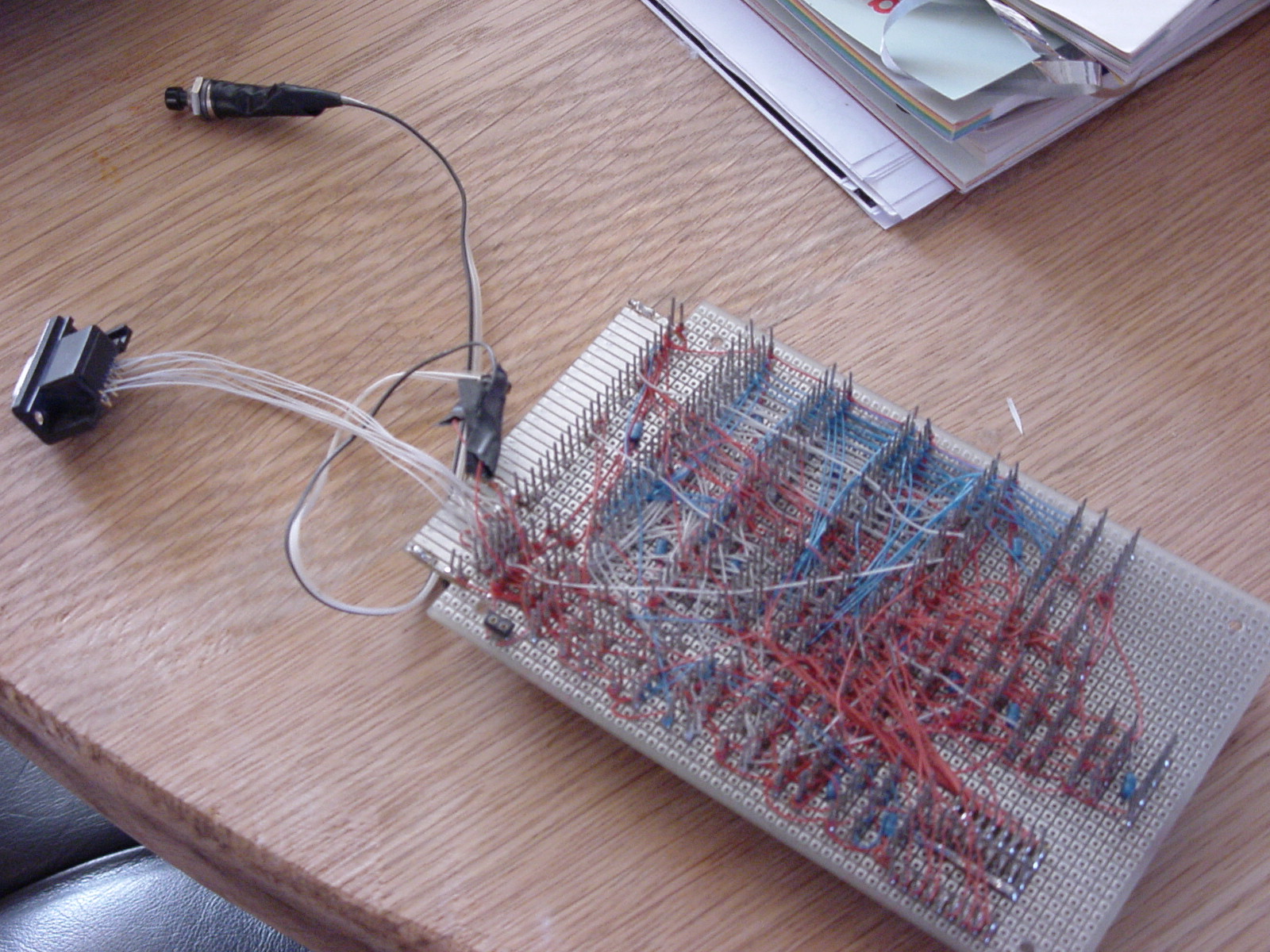
{funny story] In 2019 i wanted to make a simple probe, which could detect 0 or 1 or a pulse. I wanted to make this on a little print using wirewrap wires and IC sockets. (I still have the tool which i used in the 90s.) When going to a well-known electronics shop in Den Hague. A great shop to get all kinds of oldskool electronics. But i’m getting ahead of the story. This shop has a lot of components for all kinds of electronics. New and what it looked like de-soldered component from boards or bought from old going-out-of-business shops or factories. Stuff you needed for 60s equipment. Well i was at the counter, asking a old guy. “Do you have wire-wrap wire” He said: ” No that’s old skool” …. {/funny story]
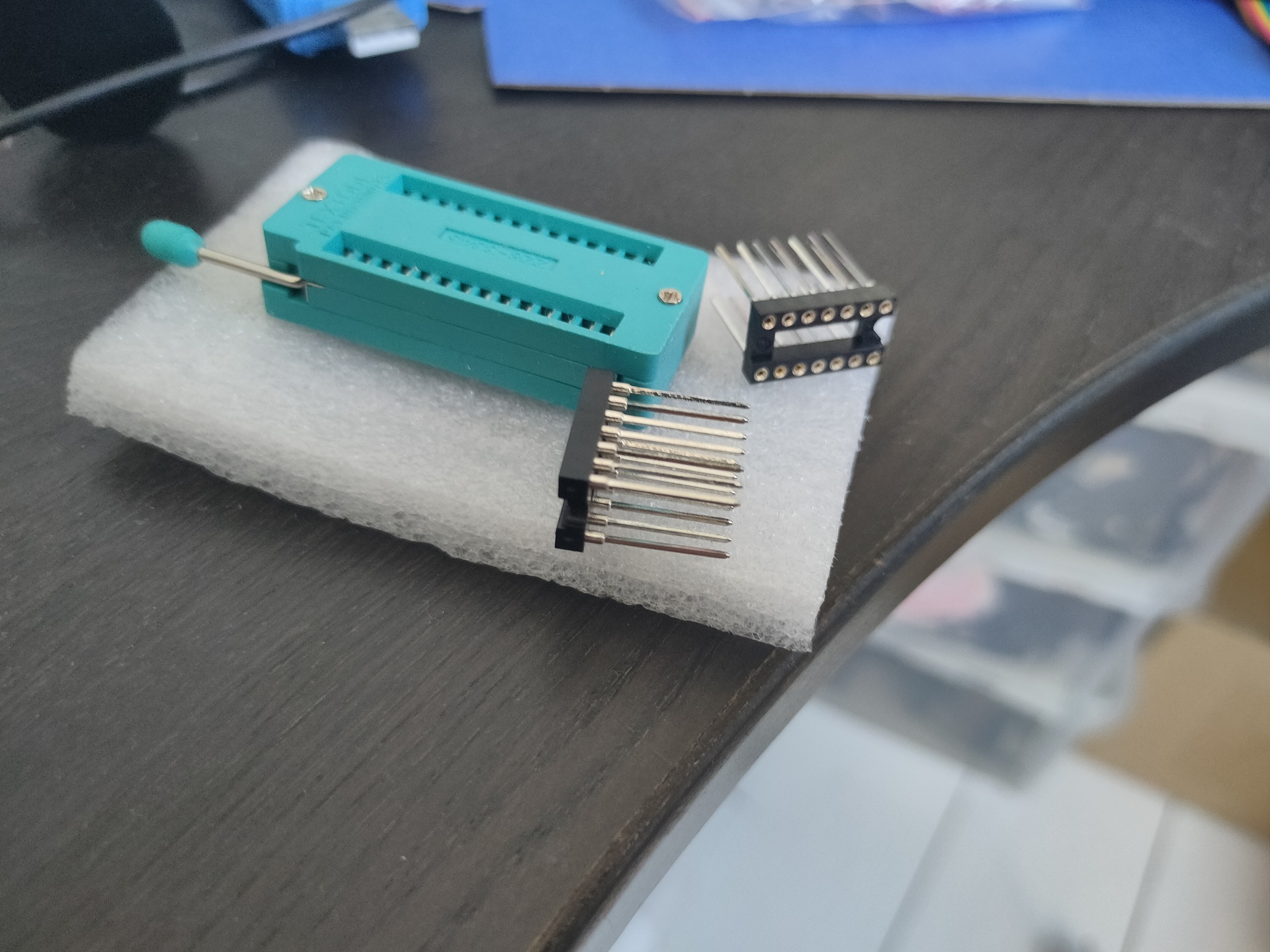
Latest wirewrap only a few years agoFrontToolsIn front the wirewrap sockets, I even had ZIF sockets (at the back) with long pins for wirewrapping.Ugly back from print
The wirewrap tool has a cable stripper. After stripping you would put a short part in the tool, place the tool over a IC pin and turning would wrap the wire on the pins. You could stack multiple connections on one pin. Removing could be done by turning the tool counterclockwise. Sometimes you had to remove the one closest to the print, replacing all wires. (Or cut the wrong/not needed wire and leave it in place … )
I’m thinking of moving my breadboard 6502 to a wirewrapped version. All my old boards are gone .. before i got a digital camera .. 🙁
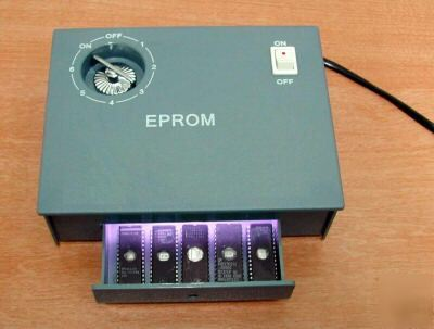
Flashing ROMs .. (eeproms). It used to be a pain in the *$$. Burning took a looong time. But clearing one with UV took .. 20 minutes or so. Using one of these:
Altered clock module
Changed button press
Dipswitches for more speed control (red .. upper left)
Changed Rom/Ram
Changed addressing
Added RAM
ZIF Socket for ROM
VIC 6522
Fixed clock
Added buttons for interrupt
Display
Display works now
To test: Create Address logic to access display without VIA Can work, but not at high speed clock. Stays behind VIA
To buy: st7920 lcd 128×64
Generic improvements
Rewired most parts, using color codes (Blue data, Yellow Address and so on)
Added leds on data and address bus using ULN2803 darlington arrays
100nF Decoupling capacitors on the power rails
To do’s or ‘have to look into’s’
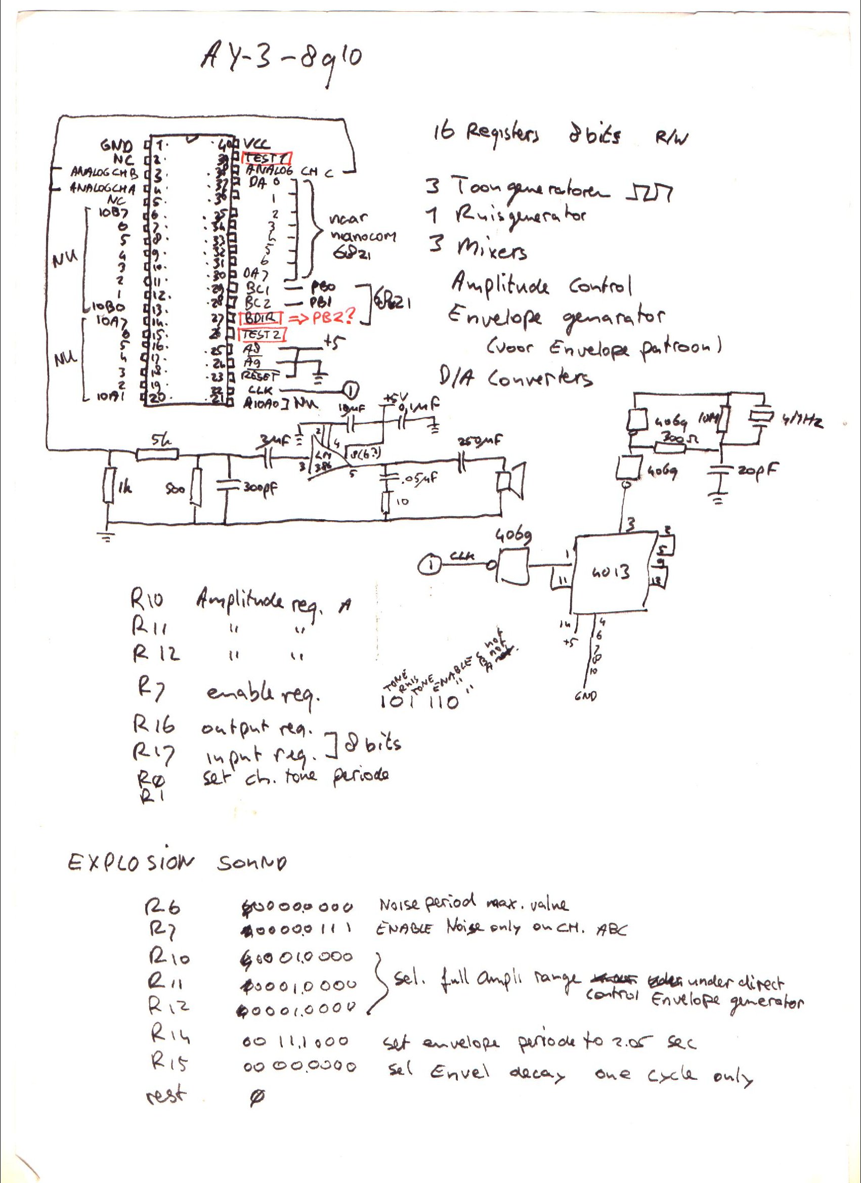
For sound i planned to use a General Instrument AY-3-8910, it is somewhere in my Lab, i know it is. I saved this chip and a SID for my Amiga addon soundcard. Where are my plans for the simple v1 setup? (FOUND IT)
I have to start writing rom functions for display usage. Like JSR $ff00 – Clear screen subroutine .. etc
I’m scraping information from websites, to get started on my clock controller. ATmega328 with ssd1306 display and rotary encoder/dip switches
Notes about the movie: Left side is Arduino IDE monitor reading Addressbus and Databus. (I’m going to try to rewrite this to realtime disassemble) Resetting system. Stepping CPU with manual clock pulses. Start vector being read at $FFFC/$FFFD. Program being run from $8000. Set clock on automatic ( ~ about 150 Hz ) Last opcodes you see a JMP loop 4C 2F 80, that is JMP $802F Display enlarged on video, was not visible on movie i took on mobile. (Wrong angle?)
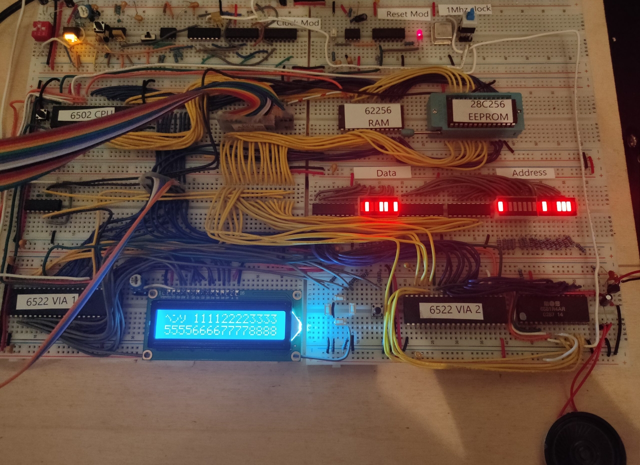
Breadboard overview
Clock module
Reset module + Crystal
CPU + nmi/int buttons
RAM and ROM
Address decode + Bus divide
Addres/Data bus leds
6522 VIA + Display
2nd via + Buttons
?
(sound board)
TIL: 6502 can run without ram only rom,expect when using JSR … which uses a program stack in RAM
TODO:
Make Clock module and 1Mhz Crystal switchable
NMI and INT debounce maken
Software buttons
Buy new darlingtons, for controlbus!
r/w, int, chip enables, etc
Labels on chips/breadboards
"If something is worth doing, it's worth overdoing."